Manufacturing method of metal-oxide-semiconductor field effect transistor (MOSFET)

An oxide semiconductor and field effect transistor technology, applied in the field of metal oxide semiconductor field effect transistor fabrication, can solve the problems of increasing the short-channel effect of the conductive channel, reducing the short-channel effect, etc., so as to avoid the short-channel effect , The effect of reducing leakage current and improving device life

Active Publication Date: 2012-05-30
SEMICON MFG INT (SHANGHAI) CORP +1
View PDF7 Cites 12 Cited by
  • Summary
  • Abstract
  • Description
  • Claims
  • Application Information

AI Technical Summary

Problems solved by technology

In the prior art, if the overall doping concentration of the conductive channel 104 is uniformly reduced in the process of ion implantation to form the conductive channel, although the GIDL can be reduced, but because the overall

Method used


Image

  • Manufacturing method of metal-oxide-semiconductor field effect transistor (MOSFET)
  • Manufacturing method of metal-oxide-semiconductor field effect transistor (MOSFET)
  • Manufacturing method of metal-oxide-semiconductor field effect transistor (MOSFET)

Examples


specific Embodiment 1

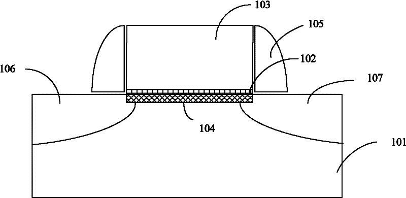
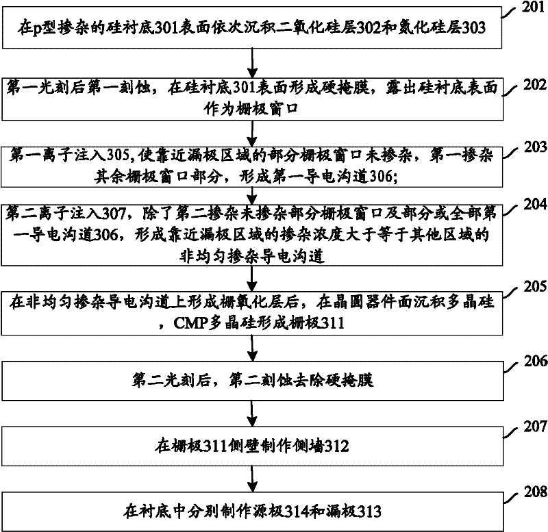
[0023] A kind of manufacture method of N-type MOSFET, below in conjunction with attached Figure 3a~3h , detailing the specific steps for fabricating N-type MOSFETs.

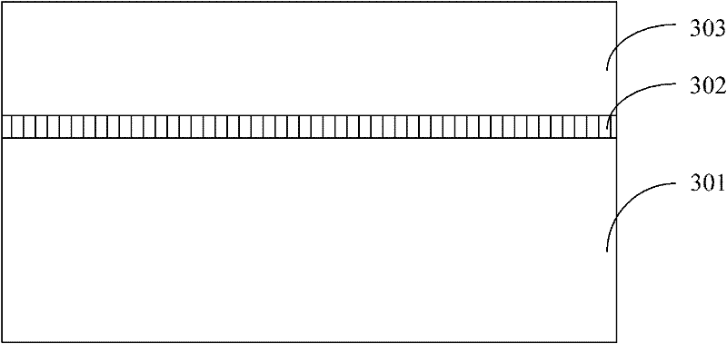
[0024] Step 201, Figure 3a It is a schematic cross-sectional structure diagram of step 201 of the N-type MOSFET manufacturing method of the present invention, such as Figure 3a As shown, a wafer with a p-type doped silicon substrate 301 is provided, a source region and a drain region are arranged in the silicon substrate 301, and a silicon dioxide layer 302 and silicon nitride are sequentially deposited on the surface of the silicon substrate 301 Layer 303;

[0025] This embodiment takes the manufacturing method of N-type MOSFET as an example, so a p-type doped silicon substrate 301 is used; if it is a manufacturing method of P-type MOSFET, an n-type doped silicon substrate is used.

[0026] In this step, the stacked structure of silicon dioxide layer 302 and silicon nitride layer 303 is used as the first d...


PUM

PropertyMeasurementUnit
Thicknessaaaaaaaaaa

Abstract

The invention provides a manufacturing method of a metal-oxide-semiconductor field effect transistor (MOSFET), comprising the following steps: manufacturing a hard mask on the surface of a silicon substrate on a source region and a drain region before a conductive channel is formed, and carrying out ion implantation at twice from different angles by using the hard mask as a shield in the process for forming the conductive channel through ion implantation to form a nonuniform conductive channel, thus, the doping concentration of the part of the conductive channel near the edge of the drain region is reduced on the premise that the whole doping concentration of the nonuniform conductive channel is not remarkably changed, on the one hand, the short channel effect of the MOSFET is prevented from increasing, and on the other hand, the band-gap tunneling effect and drain leakage current are reduced, shutdown current is reduced, and the service life of the MOSFET device is prolonged.

Description

technical field [0001] The invention relates to a semiconductor manufacturing method, in particular to a manufacturing method of a metal oxide semiconductor field effect transistor. Background technique [0002] Currently, metal-oxide-semiconductor field-effect transistor (MOSFET) device structures include: figure 1 As shown, the gate oxide layer 102 on the surface of the substrate 101, the gate 103 above the gate oxide layer 102, and the conductive channel 104 formed on the substrate surface below the gate oxide layer are respectively located in the substrate on both sides of the gate 103. A source 106 and a drain 107, and an oxynitride (silicon oxide and silicon nitride) spacer 105 (Spacer) surrounding the sidewall of the gate. On the one hand, the oxynitride spacer 105 can protect the gate 103, and on the other hand, it can prevent the source and drain implants forming the source 106 and the drain 107 from being too close to the conductive channel 104 to cause leakage cu...

Claims


Application Information

Patent Timeline
IPC IPC(8): H01L21/336H01L21/265
Inventor 刘金华
Owner SEMICON MFG INT (SHANGHAI) CORP
Why Eureka
Try Eureka