Two-bit non-volatile memory devices including independently-controllable gate electrodes and methods for fabricating the same

a non-volatile memory, gate electrode technology, applied in the direction of semiconductor devices, basic electric elements, electrical appliances, etc., can solve the problems of difficult to scale down the size of memory devices, and relatively complex peripheral circuitry

Inactive Publication Date: 2006-08-17
SAMSUNG ELECTRONICS CO LTD
View PDF13 Cites 16 Cited by
  • Summary
  • Abstract
  • Description
  • Claims
  • Application Information

AI Technical Summary

Benefits of technology

[0056] In some embodiments, during a read operation, the control voltage of about 2 V to about 6 V applied to the gate may be capacitively coupled to the channel region under the separate insulating layer, so that the channel region is in the ‘ON’ state. However, when the impurity diffusion region is formed u

Problems solved by technology

This may pose serious problems with regard to scaling down the sizes of memory devices while providing reduced price and greater density.
However, to control the three gates 45L, 45R, and 49, peripheral c

Method used


Image

  • Two-bit non-volatile memory devices including independently-controllable gate electrodes and methods for fabricating the same
  • Two-bit non-volatile memory devices including independently-controllable gate electrodes and methods for fabricating the same
  • Two-bit non-volatile memory devices including independently-controllable gate electrodes and methods for fabricating the same

Examples


Embodiment Construction

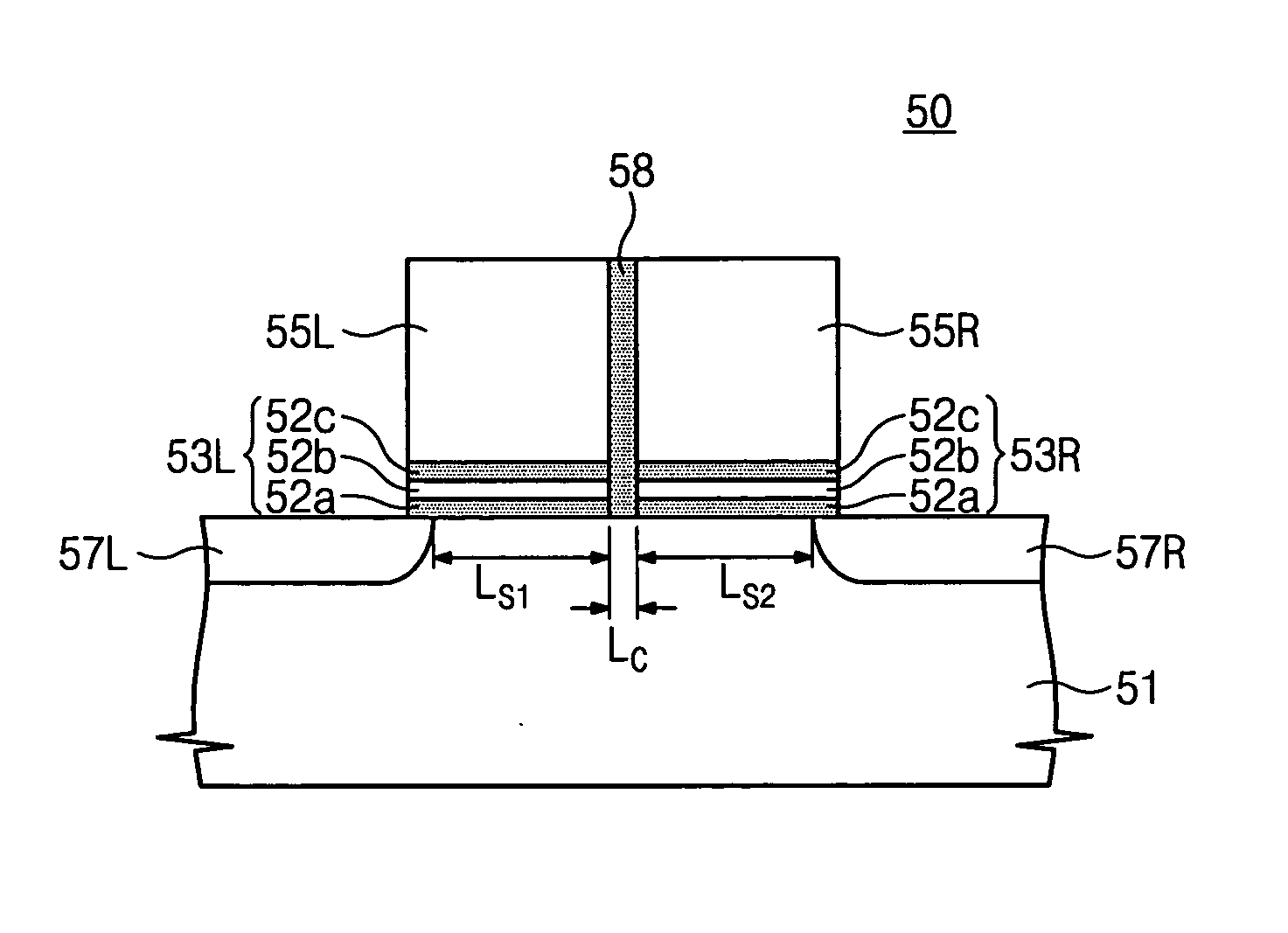
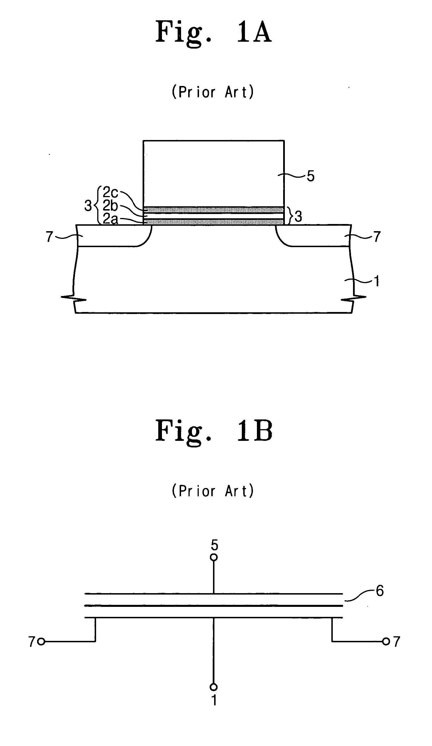
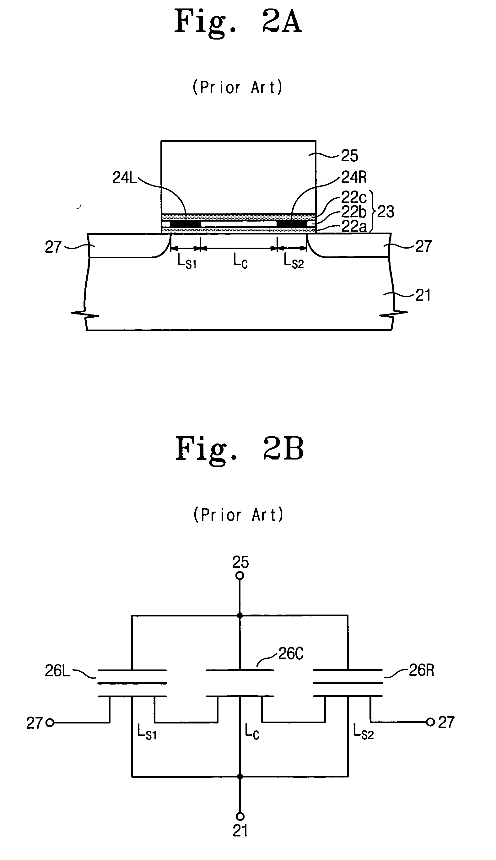
[0075] The present invention is described more fully hereinafter with reference to the accompanying drawings, in which embodiments of the invention are shown. This invention may, however, be embodied in many different forms and should not be construed as limited to the embodiments set forth herein. Rather, these embodiments are provided so that this disclosure will be thorough and complete, and will fully convey the scope of the invention to those skilled in the art. In the drawings, the size and relative sizes of layers and regions may be exaggerated for clarity. Like numbers refer to like elements throughout.

[0076] It will be understood that when an element or layer is referred to as being “on”, “connected to” or “coupled to” another element or layer, it can be directly on, connected or coupled to the other element or layer or intervening elements or layers may be present. In contrast, when an element is referred to as being “directly on,”“directly connected to” or “directly coup...


PUM


Abstract

A non-volatile integrated circuit memory device includes a substrate including first and second source/drain regions therein and a channel region therebetween, a first memory cell on the channel region adjacent the first source/drain region, and a second memory cell on the channel region adjacent the second source/drain region. The first memory cell includes a first conductive gate on the channel region and a first multi-layered charge storage structure therebetween. Similarly, the second memory cell includes a second conductive gate on the channel region and a second multi-layered charge storage structure therebetween. A single-layer insulating layer on the channel region extends between the first and second memory cells along sidewalls thereof. The single-layer insulating layer may not include a charge-trapping layer, and may separate the first and second conductive gates by a distance of less than a thickness of the first multi-layered charge storage structure. Related fabrication methods are also discussed.

Description

CROSS-REFERENCE TO RELATED APPLICATIONS [0001] The present application claims priority under 35 U.S.C. §119 from Korean Patent Application No. 10-2005-0011978, filed on Feb. 14, 2005, in the Korean Intellectual Property Office, the disclosure of which is hereby incorporated by reference herein in its entirety. FIELD OF THE INVENTION [0002] The present invention relates to semiconductor devices, and more particularly, to non-volatile memory devices and methods for fabricating the same. BACKGROUND OF THE INVENTION [0003] Generally, non-volatile memory devices, such as eraseable programmable read only memory (EPROM), electrically eraseable programmable read only memory (EEPROM), flash EEPROM, and the like, may retain stored data even without power supplied thereto. [0004] In comparison with conventional non-volatile memory devices including a floating gate, non-volatile memory devices using nonconductors (which may enable charges to be trapped locally), may offer advantages such as sim...

Claims


Application Information

Patent Timeline
IPC IPC(8): H01L29/76
CPCH01L21/28282H01L27/115H01L27/11568H01L29/513H01L29/66833H01L29/7923H01L29/40117H10B43/30H10B69/00H01L29/4234
Inventor PARK, KI-TAECHOI, JUNG-DAL
Owner SAMSUNG ELECTRONICS CO LTD
Why Eureka
Try Eureka