Magnetic field coupling element, antenna device, and electronic equipment

a magnetic field and coupling element technology, applied in the direction of resonant antennas, loop antennas with ferromagnetic cores, particular array feeding systems, etc., can solve the problems of reducing the number of resonances to be added, and reducing the coupling coefficient between the two coils. , the effect of broadening the domain in which communication is possibl

Active Publication Date: 2021-01-26
MURATA MFG CO LTD
View PDF6 Cites 0 Cited by
  • Summary
  • Abstract
  • Description
  • Claims
  • Application Information

AI Technical Summary

Benefits of technology

[0010]With the above configuration, a coupling coefficient is increased while inductances of the coils are reduced or prevented. In addition, unnecessary coupling with an electronic component or a conductor that is close to the periphery or another conductor pattern in the multi-layer body is reduced or prevented.
[0035]With the above configuration, it is not necessary to provide a conductive member or a conductor pattern that is dedicated to the radiating element, and downsizing is able to be achieved. Also in electronic equipment including a metal housing, the metal housing does not prevent the radiation of the radiating element.

Problems solved by technology

However, a radiation characteristic of the radiating elements may be degraded when an inductance component of the transformer is large because inductances (primary inductance, secondary inductance, and leakage inductance) of the transformer cause a distribution of current generated in the radiating elements to vary.
On the other hand, when the number of turns of the first coil and the second coil is decreased so as to reduce the inductance component of the transformer, a coupling coefficient between the two coils is decreased, and sufficient effects as the coupling degree adjustment circuit cannot be obtained.

Method used


Image

  • Magnetic field coupling element, antenna device, and electronic equipment
  • Magnetic field coupling element, antenna device, and electronic equipment
  • Magnetic field coupling element, antenna device, and electronic equipment

Examples


first preferred embodiment

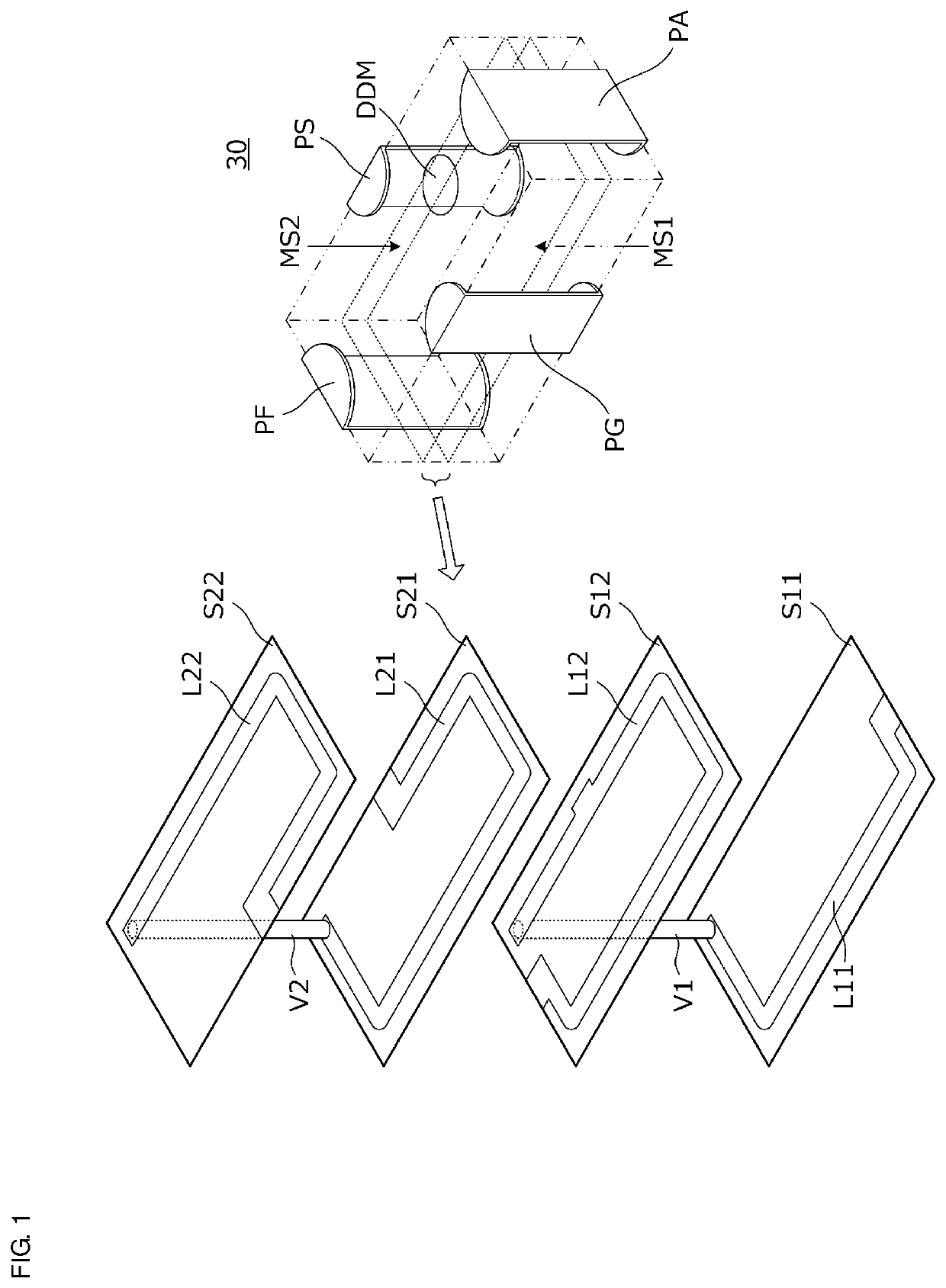
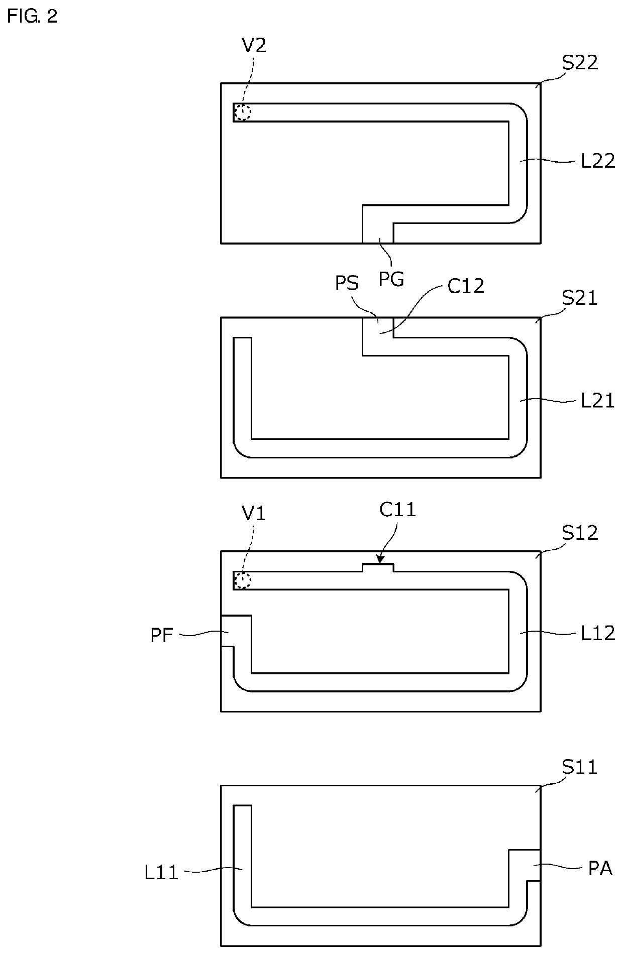
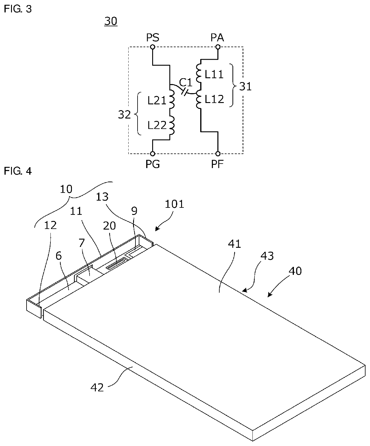
[0090]FIG. 1 is a perspective view of a coupling circuit 30 that is an example of the magnetic field coupling element according to a first preferred embodiment of the present invention. FIG. 2 is an exploded plan view illustrating conductor patterns provided on layers of the coupling circuit 30.

[0091]The coupling circuit 30 according to the present preferred embodiment is a rectangular or substantially rectangular parallelepiped chip component to be mounted on a circuit substrate in electronic equipment. In FIG. 1, an external structure of the coupling circuit 30 and an internal structure thereof are separately illustrated. The external structure of the coupling circuit 30 is represented by a two-dotted-and-dashed line. On an outer surface of the coupling circuit 30, a feeder circuit connection terminal PF, a radiating element connection terminal PA, a ground terminal PG, and a parasitic resonant circuit connection terminal PS are provided. In addition, the coupling circuit 30 inclu...

second preferred embodiment

[0143]FIG. 11 illustrates a circuit configuration of an antenna device 102 according to a second preferred embodiment of the present invention. In the antenna device 102, an inductor 35 is connected (inserted) between the second coil 32 of the coupling circuit 30 and the parasitic resonant circuit 20. The remaining configuration is the same or substantially the same as that of the circuit illustrated in FIG. 6 in the first preferred embodiment.

[0144]According to the present preferred embodiment, the inductor 35 is provided at a portion at which current is low. Thus, while a change in the coupling of the coupling circuit 30 is reduced or prevented, the resonant frequency of the parasitic resonant circuit 20 is able to be decreased, and a desired communication band is able to be obtained. Alternatively, while the resonant frequency is maintained, the length of the parasitic resonant circuit 20 is able to be reduced, and the area used is reduced.

[0145]Note that the inductor 35 may also...

third preferred embodiment

[0146]FIG. 12 illustrates a circuit configuration of an antenna device 103 according to a third preferred embodiment of the present invention. In the antenna device 103, the inductor 35 is connected (inserted) between the second coil 32 of the coupling circuit 30 and the ground. The remaining configuration is the same or substantially the same as that of the circuit illustrated in FIG. 6 in the first preferred embodiment.

[0147]When the coupling circuit 30 is added to the antenna device, a parasitic capacitance is generated between the ground and the coupling circuit 30. According to the present preferred embodiment, resonance between the inductor 35 and the parasitic capacitance is able to reduce or prevent a reactance component. Therefore, in a frequency band in which an antenna characteristic is not desired to be changed by the addition of the coupling circuit 30 to the antenna device, by including the inductor 35 with such an inductance as to resonate with the parasitic capacitan...


PUM

PropertyMeasurementUnit
inductancesaaaaaaaaaa
frequencyaaaaaaaaaa
center frequency F1aaaaaaaaaa

Abstract

A magnetic field coupling element includes conductor patterns stacked with insulating layers interposed therebetween, and interlayer connection conductors that inter-connect the conductor patterns at predetermined positions. The conductor patterns include first, second, third, and fourth conductor patterns, and the interlayer connection conductors include first and second interlayer connection conductors. The first conductor pattern, the second conductor pattern, and the first interlayer connection conductor define a first coil, and the third conductor pattern, the fourth conductor pattern, and the second interlayer connection conductor define a second coil. The first coil and the second coil are disposed in a region of less than about ⅓ of a stacking height of a multi-layer body including the insulating layers.

Description

CROSS REFERENCE TO RELATED APPLICATIONS[0001]This application claims the benefit of priority to Japanese Patent Application No. 2016-231025 filed on Nov. 29, 2016, Japanese Patent Application No. 2016-255730 filed on Dec. 28, 2016, Japanese Patent Application No. 2017-082044 filed on Apr. 18, 2017, Japanese Patent Application No. 2017-104651 filed on May 26, 2017, and Japanese Patent Application No. 2017-158219 filed on Aug. 18, 2017, and is a Continuation Application of PCT Application No. PCT / JP2017 / 042707 filed on Nov. 29, 2017. The entire contents of each of the above-identified applications are hereby incorporated herein by reference.BACKGROUND OF THE INVENTION1. Field of the Invention[0002]The present invention relates to a magnetic field coupling element that is used for a high-frequency circuit, an antenna device including the same, and electronic equipment.2. Description of the Related Art[0003]In order to broaden a frequency band or to comply with a plurality of frequency ...

Claims


Application Information

Patent Timeline
Patent Type & Authority Patents(United States)
IPC IPC(8): H01Q1/50H01Q5/335H01Q5/378H01Q21/00H01Q1/36H01Q9/30H01Q1/24H01P5/18
CPCH01Q5/335H01P5/18H01Q1/24H01Q1/36H01Q5/378H01Q9/30H01Q21/0006H01F38/14H01Q7/00H02J50/12H01Q7/06
Inventor MIKAWA, KENTAROISHIZUKA, KENICHINASU, TAKAFUMI
Owner MURATA MFG CO LTD
Why Eureka
Try Eureka