Semiconductor apparatus and method for fabricating the same

A semiconductor and pocket area technology, applied in semiconductor/solid-state device manufacturing, semiconductor devices, transistors, etc., to achieve the effects of improving short channel effects, reducing leakage current, and improving performance

Active Publication Date: 2010-12-08
TAIWAN SEMICON MFG CO LTD
View PDF0 Cites 16 Cited by
  • Summary
  • Abstract
  • Description
  • Claims
  • Application Information

AI Technical Summary

Problems solved by technology

However, these advances have also increased the complexity of the manufacturing IC process, so the IC process needs to have the same progress to achieve more advanced integrated circuit IC process

Method used


Image

  • Semiconductor apparatus and method for fabricating the same
  • Semiconductor apparatus and method for fabricating the same
  • Semiconductor apparatus and method for fabricating the same

Examples


Embodiment Construction

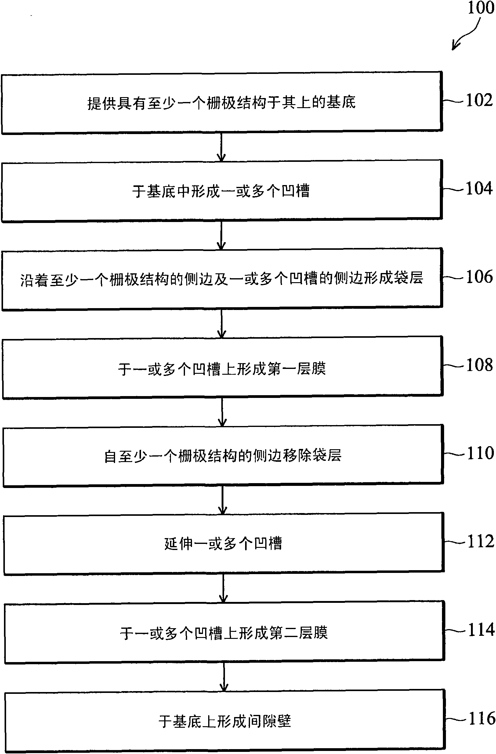
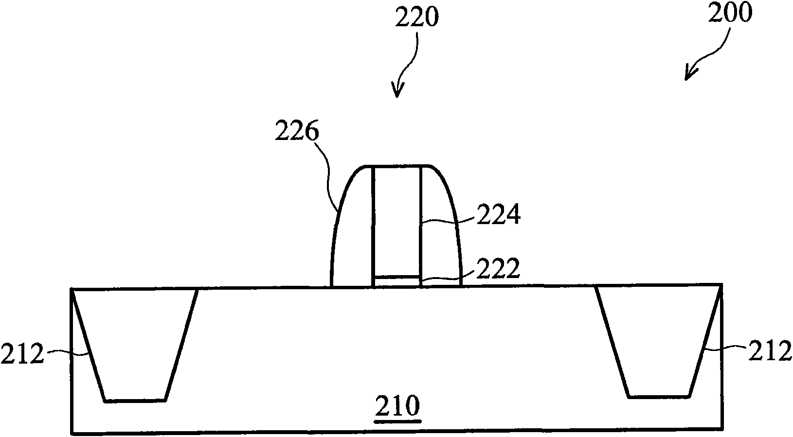
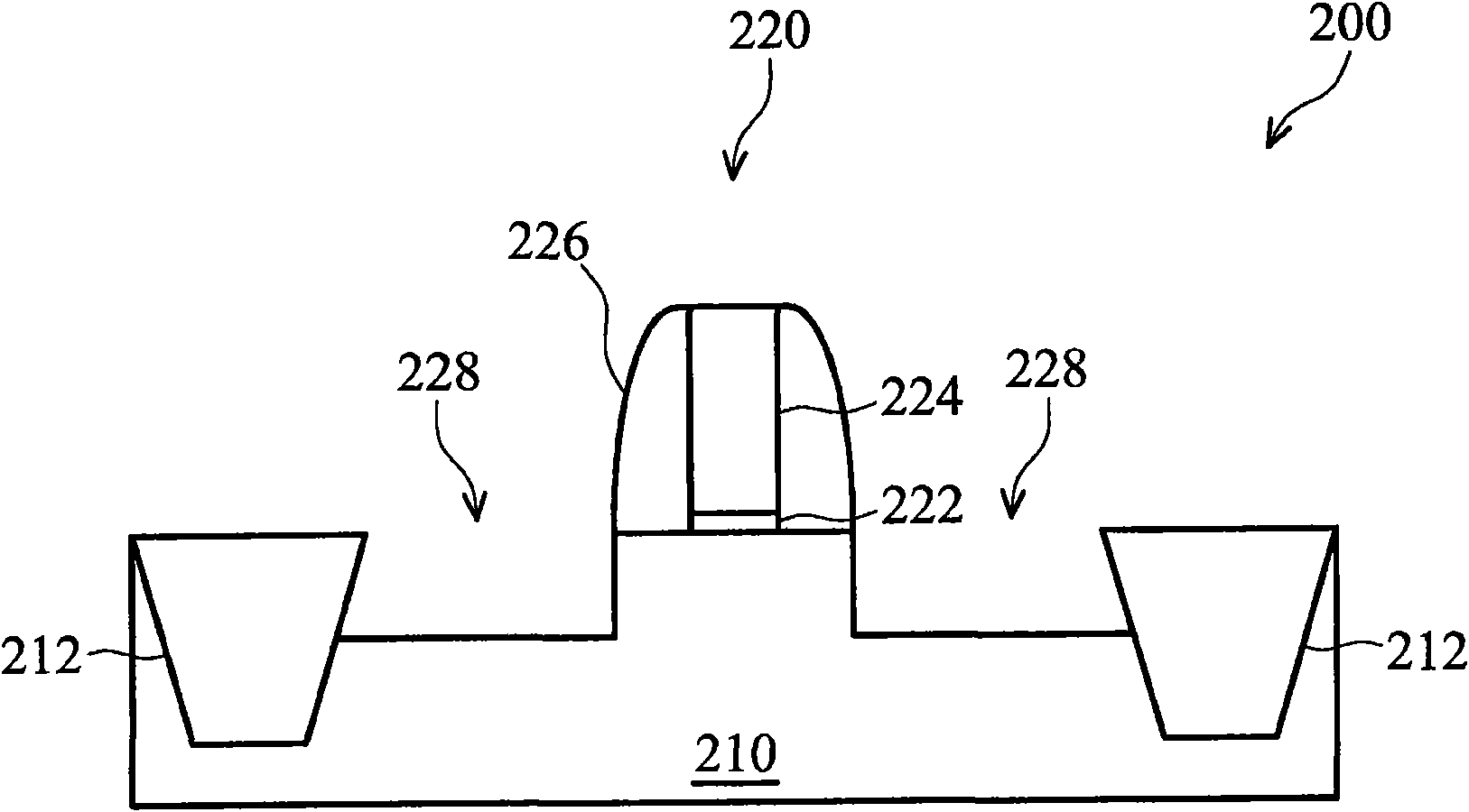
[0017] The present invention relates to a method of manufacturing a semiconductor device, in particular to a method of manufacturing a semiconductor device that improves device performance and / or improves control of short channel effects. The manner in which various embodiments can be made and used is described in detail below. However, it should be noted that the various applicable inventive concepts provided by the present invention are implemented according to various changes in the specific context, and the specific embodiments discussed here are only used to show the specific use and manufacture The method of the present invention is not intended to limit the scope of the present invention. The following is a description of the manufacturing process of the preferred embodiment of the present invention through various drawings and examples. In the various and various embodiments of the invention and in the drawings, the same reference numerals represent the same or simila...


PUM


Abstract

The invention provides a semiconductor apparatus and method for fabricating the same. The method comprises providing a substrate comprising a first material; forming at least one gate stack over the substrate; forming one or more recesses in the substrate, wherein the one or more recesses define at least one source region and at least one drain region; and forming a pocket, a first layer comprising a second material, and a second layer comprising a third material in the one or more recesses, the pocket being disposed between the first layer and the substrate. The pockets 234 of the invention,essentially providing an abrupt junction between the source / drain region and substrate interface, may lead to significant improvement in SCEs (short channel effect) and / or reduce current leakage. Improvement in SCEs can allow continual semiconductor device scaling down. Further, in the present embodiment, the method may reduce strain relaxation within the SiGe portions of the source / drain regions, which can improve the performance of semiconductor device. the invention also reduces the channel doping degree.

Description

technical field [0001] The present invention relates to a manufacturing method of a semiconductor device, in particular to a manufacturing method of a semiconductor device related to improving device performance and / or improving control of short channel effect. Background technique [0002] The semiconductor integrated circuit (IC) industry has experienced rapid growth. Technological advances in IC materials and design have resulted in successive generations of IC production, each with smaller and more complex circuits than the previous generation. However, these advances have also increased the complexity of the manufacturing IC process, so the IC process also needs to have the same progress in order to achieve a more advanced integrated circuit IC process. [0003] In the course of IC innovation, functional density (ie, the number of interconnected devices per wafer area) has generally increased, while geometry size (ie, the smallest element (or line) that can be created ...

Claims


Application Information

Patent Timeline
Patent Type & Authority Applications(China)
IPC IPC(8): H01L21/8234H01L21/336H01L27/088H01L29/78H01L29/06
CPCH01L21/823807H01L29/7833H01L21/823814H01L29/7848H01L29/0653H01L29/66636H01L29/165H01L29/6659H01L29/6653
Inventor 官大明柯志欣李文钦
Owner TAIWAN SEMICON MFG CO LTD
Why Eureka
Try Eureka