Extended drain transistor and method of manufacturing the same

a technology of extended drain transistor and manufacturing method, which is applied in the direction of basic electric elements, electrical apparatus, and semiconductor devices, can solve the problems of failure of conventional transistor manufacturing procedures, and achieve the effects of reducing electric field, simple and efficient way, and proper performan

Active Publication Date: 2012-07-10
NXP BV
View PDF10 Cites 4 Cited by
  • Summary
  • Abstract
  • Description
  • Claims
  • Application Information

AI Technical Summary

Benefits of technology

[0021]According to an exemplary embodiment of the invention, a self-aligned EDMOS formation may be provided so that a self-aligned asymmetrically MOS device containing gate oxides and at least one drain extension may be provided. According to an exemplary embodiment, a single poly gate may be used for manufacturing such an asymmetrical field effect transistor. Particularly, the asymmetrical transistor according to an exemplary embodiment of the invention may be appropriate for small poly gate lengths, particularly below 100 nm. By taking this measure, a lower doping at the drain side may lower undesired hot carrier effects.
[0048]A width of the second spacer may be larger than the lithography overlay of a CMOS process technology used for forming the gate (see FIG. 10). By taking this measure, the dimension of the extended drain may be adjusted accurately.

Problems solved by technology

However, conventional transistor manufacture procedures may fail when the dimensions become smaller and smaller.

Method used


Image

  • Extended drain transistor and method of manufacturing the same
  • Extended drain transistor and method of manufacturing the same
  • Extended drain transistor and method of manufacturing the same

Examples


Embodiment Construction

[0062]The illustration in the drawing is schematical. In different drawings, similar or identical elements are provided with the same reference signs.

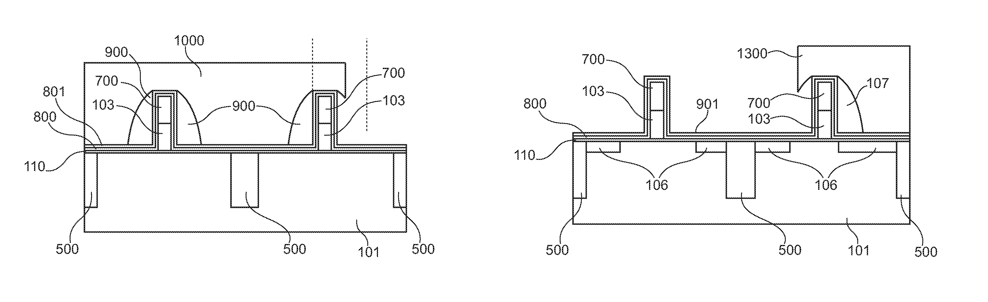
[0063]In the following, referring to FIG. 1, an EDMOS transistor 100 according to an exemplary embodiment of the invention will be explained.

[0064]The EDMOS transistor 100 is monolithically integrated in a silicon substrate 101. The silicon substrate 101 may be essentially free of any dopant or may be intrinsically doped to thereby form a channel region 102 in a central portion thereof.

[0065]The EDMOS transistor 100 further comprises a poly silicon gate 103 formed on the silicon substrate 101, wherein the gate 103 has a first vertical side wall 104 and has a second vertical side wall 105 opposing the first side wall 104. The EDMOS transistor 100 comprises an extended drain region 106, that is a region with a low dopant concentration, implanted in a surface portion of the silicon substrate 101 directly adjacent the second side wall 105 ...


PUM


Abstract

An extended drain transistor (100) comprising a substrate (101), a gate (103) formed on the substrate (100), the gate (103) having a first side wall (104) and a second side wall (105) opposing the first side wall (104), an extended drain (106) implanted in a surface portion of the substrate (101) adjacent the second side wall (105) of the gate (103), a spacer (107) on the second side wall (105) of the gate (103), a source (108) implanted in a surface portion of the substrate (101) adjacent the first side wall (104) of the gate (103), and a drain (109) implanted in a surface portion of the substrate (101) adjacent the spacer (107) in such a manner that the extended drain (106) is arranged between the gate (103) and the drain (109).

Description

FIELD OF THE INVENTION[0001]The invention relates to an extended drain transistor.[0002]Moreover, the invention relates to a method of manufacturing an extended drain transistor.[0003]Beyond this, the invention relates to an RF circuit.BACKGROUND OF THE INVENTION[0004]In semiconductor technology, the efficient manufacture of MOS transistors is essential. Particularly for RF applications, the demand on the quality of transistors increases.[0005]U.S. Pat. No. 5,828,104 discloses a MOS semiconductor device containing a MOSFET with an asymmetric LDD structure, which has in a semiconductor substrate a first heavily doped region, a lightly doped region formed adjacent to the first heavily doped region, and a second heavily doped region formed apart from the first lightly doped region. The first heavily doped region and the lightly doped region act as a drain region of the MOSFET, and the second heavily doped region acts as a source region thereof. A gate electrode composed of a plurality ...

Claims


Application Information

Patent Timeline
Patent Type & Authority Patents(United States)
IPC IPC(8): H01L21/336
CPCH01L21/823418H01L21/823468H01L29/6653H01L29/6656H01L29/66659H01L29/7835H01L29/0847Y10S257/90
Inventor MEUNIER-BELLARD, PHILLIPPEHERINGA, ANCO
Owner NXP BV
Why Eureka
Try Eureka