Structure and manufacturing method of terminal voltage-division region for super-junction device

A technology of super junction device and voltage division area, which is applied in semiconductor/solid-state device manufacturing, semiconductor devices, electrical components, etc. It can solve problems such as large interface charges, reduce breakdown voltage, and affect voltage division effect, so as to achieve voltage division effect Good, reduce the electric field intensity, improve the effect of device reliability

Active Publication Date: 2017-01-11
FOUNDER MICROELECTRONICS INT
View PDF3 Cites 4 Cited by
  • Summary
  • Abstract
  • Description
  • Claims
  • Application Information

AI Technical Summary

Problems solved by technology
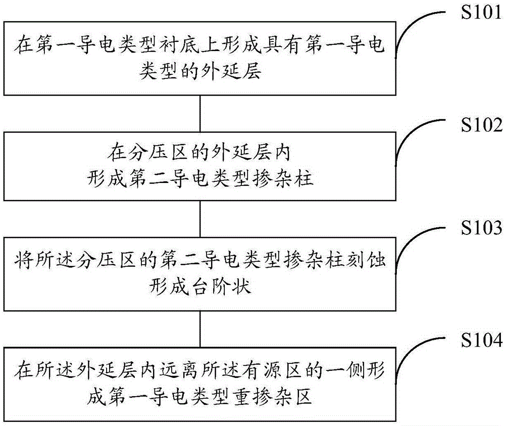
[0004] In order to solve the problem that the terminal structure of the traditional super junction device will generate a large amount of interface charge, affect the voltage division effect, and reduce the breakdown voltage, the invention provides a method and structure for manufacturing an epitaxial wafer for a super junction device

Method used


Image

  • Structure and manufacturing method of terminal voltage-division region for super-junction device
  • Structure and manufacturing method of terminal voltage-division region for super-junction device
  • Structure and manufacturing method of terminal voltage-division region for super-junction device

Examples


Embodiment 1

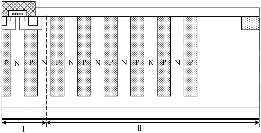
[0033] The following takes N-type super junction devices as an example to introduce the working principle of super junction devices, such as figure 1 The structure of a super-junction device shown includes an active region I and a terminal region II, both of which are alternating P-column and N-column structures.

[0034] Ⅰ. Active area:

[0035] When the device is turned off, that is, when the voltage of the gate is 0, two reverse biased PN junctions are formed laterally, the left P column and the middle vertical conductive N column form a PN junction reverse bias, and the right P column and the middle The vertical conductive N-column forms a PN junction reverse bias, the depletion layer of the PN junction increases, and a horizontal electric field is established; when the doping concentration and width are properly controlled, the middle N-column can be completely depleted, so that in the middle The N-pillar has no free charge, which is equivalent to an intrinsic semiconduc...

Embodiment 2

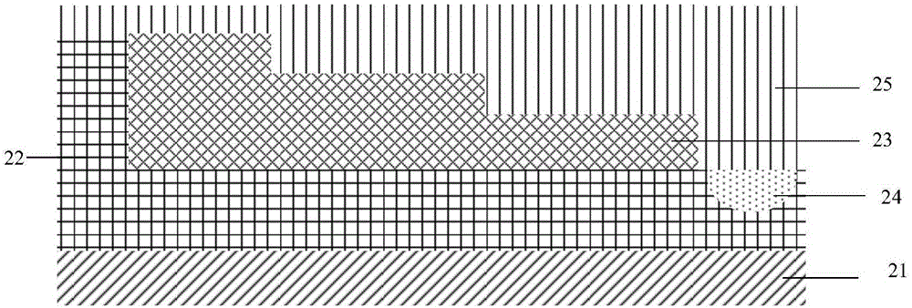
[0041] Such as figure 2 As shown, the structure of a terminal voltage division region of a super junction device provided by Embodiment 2 of the present invention includes:

[0042] a first conductivity type substrate 21;

[0043] an epitaxial layer 22 of the first conductivity type disposed on the substrate 21 of the first conductivity type;

[0044] The epitaxial layer 22 is provided with a second conductivity type doped column 23 in the voltage dividing region, and the second conductivity type doped column 23 in the voltage division region is not in contact with the second conductivity type doped column in the active region , the doped column 23 of the second conductivity type in the voltage dividing region is stepped, and the vertical height of the step decreases one by one from one end close to the active region to one end far away from the active region;

[0045] The side of the epitaxial layer away from the active region is provided with a heavily doped region 24 of ...

Embodiment 3

[0062] The following takes an N-type semiconductor as an example to describe in detail the manufacturing process of the voltage dividing region at the end of the super junction device provided by the embodiment of the present invention. Such as Figure 4 (a) ~ 4 (g) As shown in FIG. 2 , it is a schematic structural diagram of each stage in the manufacturing process of the epitaxial wafer for super-junction devices disclosed in Embodiment 2 of the present invention.

[0063] In the first step, as shown in Fig. 4(a), an N-type silicon single wafer is used as the substrate 1, and the front side of the single wafer is cleaned.

[0064] In the second step, as shown in FIG. 4( b ), an N-type epitaxial layer 2 is grown on the substrate 1 , and P columns 3 are formed in the N-type epitaxial layer 2 .

[0065] Here, the P column 3 and the P column in the active region are formed simultaneously by the same process, multiple epitaxial implantation techniques can be used, and the formed ...


PUM


Abstract

The invention relates to a semiconductor manufacturing field, particularly to a structure and a manufacturing method of a terminal voltage-division region for a super-junction device. The structure of the terminal voltage-division region comprises a first conductive type substrate, and a first conductive type epitaxial layer which is arranged on the first conductive type substrate, wherein a second conductive type doped column in a voltage-division region is arranged in the epitaxial layer; the second conductive type doped column in the voltage-division region is not in contact with a second conductive type doped column in an active region; the second conductive type doped column in the voltage-division region is stage-shaped; the vertical heights of the stages are reduced one by one in sequence from one end close to the active region to one end far from the active region; a first conductive type heavily-doped region is arranged on one side, far from the active region, in the epitaxial layer; and the heavily-doped region is not in contact with the second conductive type doped column in the voltage-division region. By adoption of the structure and the manufacturing method of the terminal voltage-division region for the super-junction device, the problems of influence to a voltage-division effect and reduction of breakdown voltage caused by a conventional terminal structure for the super-junction device due to a large amount of generated interface charges are solved.

Description

technical field [0001] The invention relates to the field of semiconductor manufacturing, in particular to a structure and a manufacturing method of a terminal voltage division region of a super junction device. Background technique [0002] Super-junction metal-oxide-semiconductor field-effect transistors (MOSFETs) have higher breakdown voltage and lower on-resistance than conventional power devices. Super-junction MOSFETs use alternating P-column and N-column structures instead of a single conductivity type material in traditional power devices as a voltage sustaining layer. A lateral electric field is introduced in the drift region, and the P-column and N-column meet the charge balance conditions. Under the bias voltage, the P-column and N-column will be completely depleted. Only when the external voltage is greater than the internal lateral electric field can this area be broken down. Therefore, the withstand voltage of this area is extremely high, so as to increase the ...

Claims


Application Information

Patent Timeline
Patent Type & Authority Applications(China)
IPC IPC(8): H01L29/06H01L21/04
CPCH01L21/04H01L29/0634
Inventor 李理马万里赵圣哲
Owner FOUNDER MICROELECTRONICS INT
Why Eureka
Try Eureka