Semiconductor integrated circuit

a technology of integrated circuits and semiconductors, applied in the direction of semiconductor devices, electrical apparatus, transistors, etc., can solve the problems of failure or breakdown of hvic b, malfunction and/or breakdown due to latch-up, inversion of output logic, etc., to prevent malfunction or breakdown, the effect of preventing malfunction or breakdown

Active Publication Date: 2015-12-17
FUJI ELECTRIC CO LTD
View PDF5 Cites 17 Cited by
  • Summary
  • Abstract
  • Description
  • Claims
  • Application Information

AI Technical Summary

Benefits of technology

[0054]In order to solve the aforementioned problem inherent in the related art, an object of the invention is to provide a high voltage integrated circuit which can prevent malfunction or breakdown.
[0059]According to the aforementioned configuration, the second-conductivity-type semiconductor region fixed to the second potential (or potential of an internal power supply or a voltage division point of a voltage division resistor) higher than the first potential is formed between the pn junction area which is located between the first area constituting the high voltage junction terminal region surrounding the high side second circuit and the first-conductivity-type well region, and the first potential (lowest potential) first-conductivity-type semiconductor region which is formed in the first-conductivity-type well region. Accordingly, electrons flowing into the low side first circuit area can be extracted from the second-conductivity-type semiconductor region toward the second electrode by an operation of a parasitic diode (a parasitic pn junction area including the first area and the first-conductivity-type well region) generated when a negative surge voltage occurs (when the fourth potential or the third potential becomes negative). Thus, it is possible to prevent malfunction or breakdown due to latch-up in the logic portion of the low side first circuit connected to the first potential terminal and the second potential terminal (or the internal power supply or the voltage division point of the voltage division resistor).
[0060]In addition, according to the aforementioned configuration, the portion of the first-conductivity-type well region right under the second-conductivity-type semiconductor region whose potential is fixed to the second potential higher than the first potential serves as a pinch resistor. Accordingly, anode resistance of a parasitic diode having the first potential first-conductivity-type well region as an anode and the fourth potential second-conductivity-type well region (the second second-conductivity-type well region and the first portion) as a cathode increases when a negative surge voltage occurs. Thus, the injection amount of holes flowing into the high side second circuit connected to the fourth potential terminal and the third potential terminal can be reduced so that malfunction or breakdown due to latch-up in the second circuit can be prevented.
[0061]According to the semiconductor integrated circuit according to the invention, it is possible to obtain an effect to prevent malfunction or breakdown of the high side control circuit or the low side control circuit portion.

Problems solved by technology

As a result, there is a fear that malfunction or latch-up occurring in the high side control circuit constituting the HVIC 180 may lead to failure or breakdown in the HVIC 180.
However, the aforementioned HVIC according to the related art has the following problems.
It is because, when the minority carriers are injected into the high side control circuit and / or the low side control circuit portion, in the HVIC, a malfunctions and / or breakdown due to latch-up occur caused by a parasitic operation of the CMOS circuit constituting the logic portion of the high side control circuit and / or the low side control circuit.
Therefore, there is a fear that malfunction such as inversion of the output logic of the L-OUT etc. may be caused or breakdown due to latch-up in the low side control circuit 181 may be caused.
Therefore, there is a fear that malfunction or breakdown due to latch-up may occur in the logic portion of the high side control circuit 182.

Method used


Image

  • Semiconductor integrated circuit
  • Semiconductor integrated circuit
  • Semiconductor integrated circuit

Examples


embodiment 1

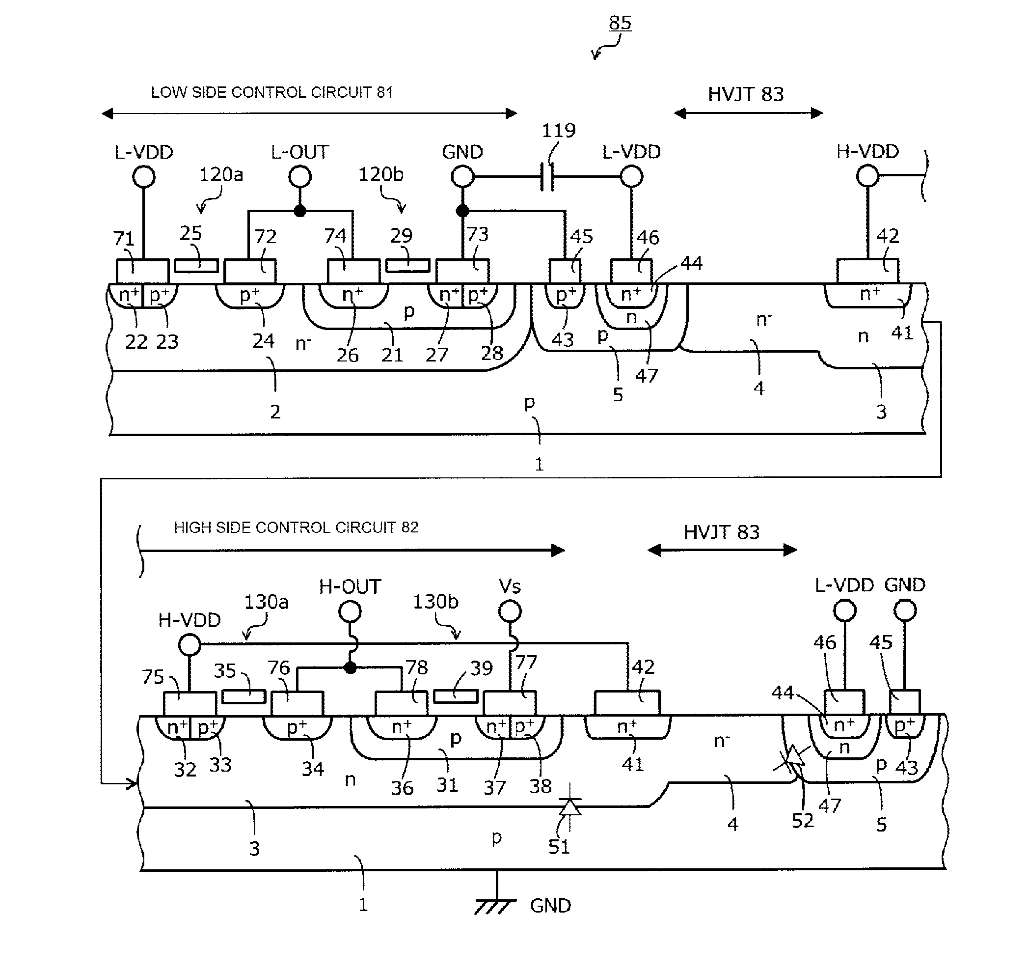
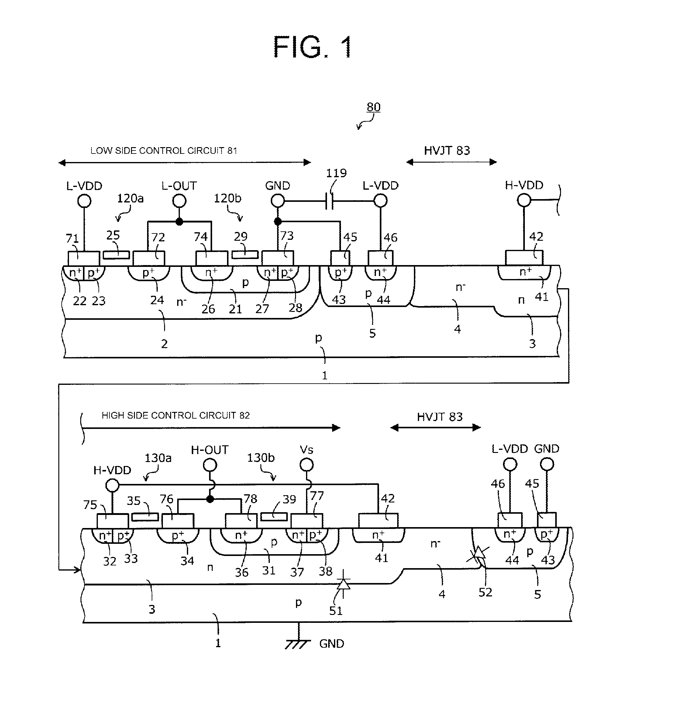
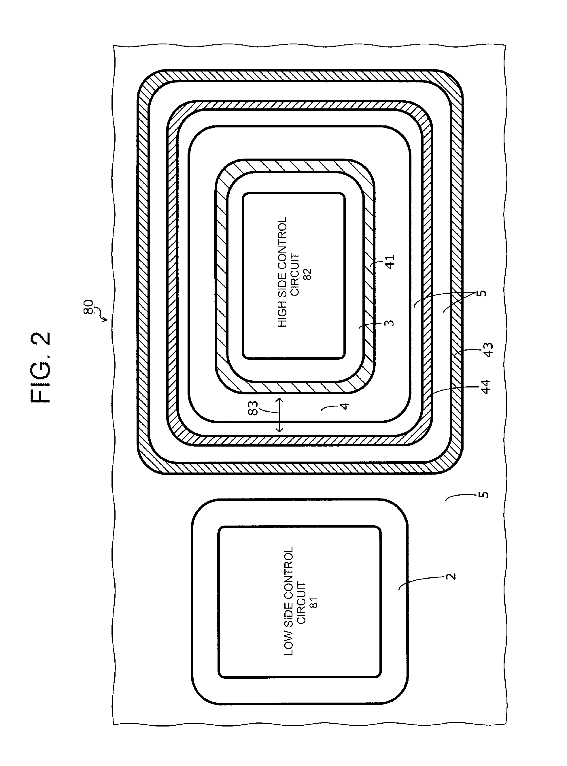
[0074]The structure of a semiconductor integrated circuit according to Embodiment 1 will be described using a self-isolation type high voltage integrated circuit (HVIC) as an example with reference to FIGS. 1, 2 and 7 to 9. FIG. 1 is a sectional view showing the sectional structure of the high voltage integrated circuit according to Embodiment 1. FIG. 2 is a plan view showing the planar structure of the high voltage integrated circuit in FIG. 1. An HVIC 80 according to Embodiment 1 is a drive element corresponding to the HVIC constituting the power conversion device shown in FIG. 7. The HVIC 80 has a function to control ON / OFF of IGBTs 114 and 115 of a half-bridge circuit.

[0075]The connection configuration of the HVIC 80 (the circuit configuration of the power conversion device), the circuit configuration of a level shift function (level shift circuit) of the HVIC 80, and a method performed by the HVIC 80 for driving the IGBTs 114 and 115 are the same as those in the related art. Th...

embodiment 2

[0105]Next, the structure of a semiconductor integrated circuit (HVIC) according to Embodiment 2 will be described. FIG. 4 is a sectional view showing the structure of a main part of the high voltage integrated circuit according to Embodiment 2. An HVIC 84 according to Embodiment 2 is different from the HVIC according to Embodiment 1 in the point that a plurality of n+ type contact regions 44 connected to higher potential than the potential of the GND are disposed in the p type well region 5 in parallel with one another in a direction from the n− type well region 4 toward the outside (p type well region 5 side). That is, two or more n+ type contact regions 44 each having a planar shape of a rectangular ring are formed in the p type well region 5 to surround the circumference of the n− type well region 4 (HVJT 83) doubly or more. FIG. 4 shows the case where, for example, three n+ type contact regions 44 are disposed.

[0106]Specifically, the n+ type contact regions 44 are disposed sepa...

embodiment 3

[0109]Next, the structure of a semiconductor integrated circuit (HVIC) according to Embodiment 3 will be described. FIG. 5 is a sectional view showing the structure of a main part of the high voltage integrated circuit according to Embodiment 3. An HVIC 85 according to Embodiment 3 is different from the HVIC according to Embodiment 1 in the point that an n type buffer region 47 having a shallower diffusion depth than the p type well region 5 is formed to cover the lower side (substrate back side) of an n+ type contact region 44 connected to higher potential than the potential of the GND. Specifically, the n type buffer region 47 is selectively formed in a front surface layer of a substrate back side of the p type well region 5, and the n+ type contact region 44 is selectively formed inside the n type buffer region 47.

[0110]In the HVIC 85 according to Embodiment 3, a portion of the p type well region 5 right under the n type buffer region 47 becomes a pinch resistor. The diffusion de...


PUM


Abstract

A low side control circuit and a high side control circuit are disposed in first and second n type well regions, respectively. A third n type well region is formed around the second n type well region. The first n− type well region is formed outside the second n− type well region. A p type well region is formed around the third n− type well region. The third n− type well region and the p type well region constitute an HVJT between the first and second n type well regions. A p+ type contact region and a first electrode supplied with GND potential are formed in the p type well region. In the p type well region, an n+ type contact region and a second electrode supplied with L-VDD potential higher than the GND potential are formed between the HVJT and the p+ type contact region.

Description

BACKGROUND OF THE INVENTION[0001]1. Field of the Invention[0002]The present invention relates to a semiconductor integrated circuit.[0003]2. Description of the Related Art[0004]An HVIC (High Voltage Integrated Circuit) has been well known as a semiconductor integrated circuit which drives and turns ON / OFF a switching power device constituting an upper arm of a bridge circuit for power reverse conversion (DC-to-AC conversion) of a PWM (Pulse Width Modulation) inverter etc. Recently, an element separation type HVIC which does not perform potential insulation by means of a transformer, a photocoupler, etc. but uses high voltage junction has been used in order to enhance a function to perform overcurrent detection and temperature detection when the switching power device is abnormal and in order to reduce the size and cost of a power supply system.[0005]An HVIC which drives IGBTs (Insulated Gate Bipolar Transistors) used as switching power devices constituting a power conversion device ...

Claims


Application Information

Patent Timeline
Patent Type & Authority Applications(United States)
IPC IPC(8): H01L27/092
CPCH01L27/0921H01L21/761H01L21/823892
Inventor YAMAJI, MASAHARU
Owner FUJI ELECTRIC CO LTD
Why Eureka
Try Eureka