Preparation method of N-type battery and selective emitter of N-type battery, and N-type battery

A selective and emitter technology, applied in circuits, photovoltaic power generation, electrical components, etc., can solve the problems of heavy boron doping of N-type batteries, successful reports of no laser doping, etc., and achieve the effect of increasing the open circuit voltage

Active Publication Date: 2020-05-05
JA SOLAR TECH YANGZHOU +1
View PDF11 Cites 4 Cited by
  • Summary
  • Abstract
  • Description
  • Claims
  • Application Information

AI Technical Summary

Problems solved by technology

[0005] However, for heavy doping of boron in N-type

Method used


Image

  • Preparation method of N-type battery and selective emitter of N-type battery, and N-type battery
  • Preparation method of N-type battery and selective emitter of N-type battery, and N-type battery
  • Preparation method of N-type battery and selective emitter of N-type battery, and N-type battery

Examples


preparation example Construction

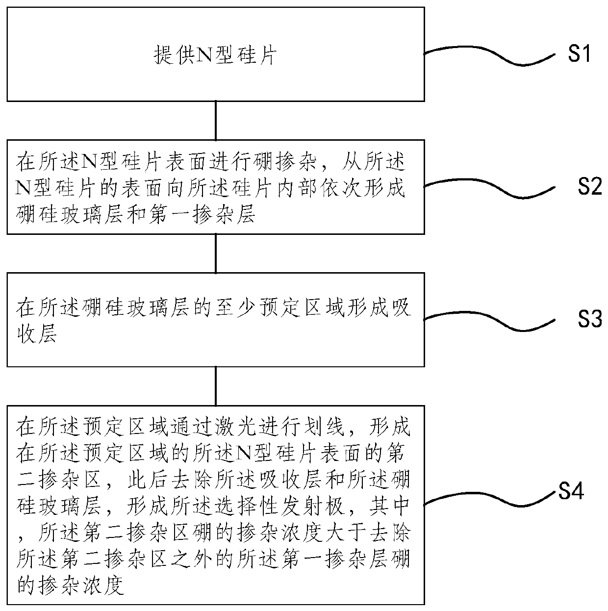
[0038] The preparation method of the N-type battery selective emitter according to the optional embodiment of the present invention, such as figure 1 shown, including the following steps:

[0039] In step S1, an N-type silicon wafer 1 is provided.

[0040] The so-called N-type silicon wafer is doped on the silicon substrate, such as the N-type silicon wafer formed by phosphorus atoms. The ability of impurities in N-type silicon wafers to capture minority carrier holes is lower than that of impurities in P-type silicon wafers to capture minority carrier electrons. The minority carrier lifetime of N-type silicon wafers with the same resistivity is 1 higher than that of P-type silicon wafers. ~2 orders of magnitude, reaching the millisecond level, and the surface recombination rate of minority carrier holes in N-type materials is lower than that of electrons in P-type materials, so N-type silicon wafers can be used to prepare cells with higher photoelectric conversion efficiency...

Embodiment 1

[0065] S11 provides N-type monocrystalline silicon wafers, the thickness of which is 150 microns, and the resistivity is 1 ohm*cm.

[0066] S12, cleaning and chemically etching the N-type silicon wafer 1 to form a textured structure.

[0067] S21, placing the N-type silicon wafer 1 in a diffusion furnace.

[0068] S22, heating up to a diffusion temperature of 960°C.

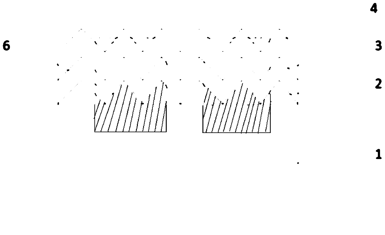
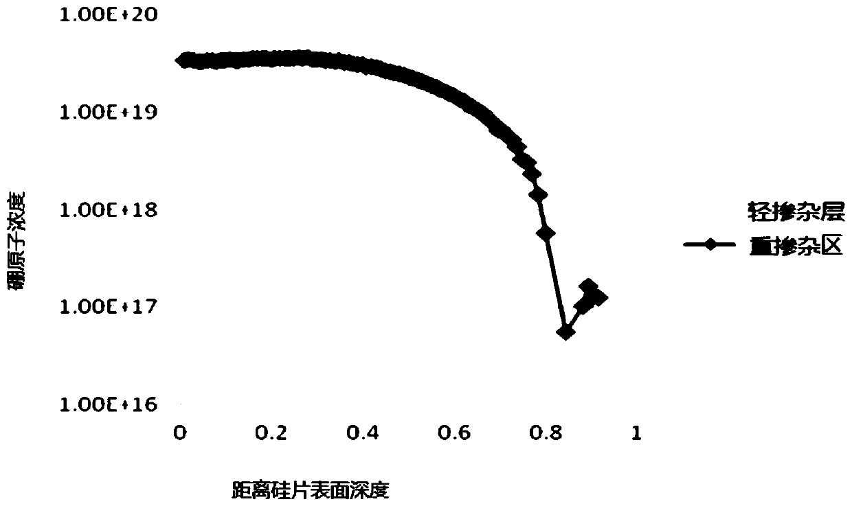
[0069] S23, pass nitrogen gas, oxygen gas (2000 sccm), and boron source nitrogen gas in the diffusion furnace, and diffuse for 40 minutes to form the first doped layer (lightly doped layer) 2 and borosilicate with a square resistance of 120 ohms / □ Glass layer 3.

[0070] S31, forming a silicon nitride layer on the surface of the borosilicate glass layer 3 by plasma chemical vapor deposition. The silicon nitride layer is the absorbing layer 4 with a thickness of 75 nm and a refractive index of 2.2.

[0071] S41, scribing lines on the surface of the absorbing layer 4 with a laser, the wavelength of the laser is ...

Embodiment 2

[0075] S11', provide N-type single crystal silicon wafer, the thickness of the silicon wafer is 200 microns, and the resistivity is 3 ohm*cm.

[0076] S12', cleaning and chemically etching the N-type silicon wafer 1 to form a textured structure.

[0077] S21', using atmospheric pressure chemical vapor deposition on the N-type silicon wafer 1 to form the above-mentioned doping source layer and covering layer to form boron oxide (doping source layer) and silicon oxide layer (covering layer) sequentially, wherein the oxide The thickness of the boron layer was 50 nm, the atomic ratio of boron was 3%, and the thickness of the silicon oxide film was 40 nm.

[0078] S22' Put the N-type silicon wafer 1 into a nitrogen atmosphere for annealing, wherein the annealing temperature is 970 degrees, and the time is 50 minutes to form the first doped layer (lightly doped layer) 2 and borosilicate glass layer 3 .

[0079] S31', on the surface of the borosilicate glass layer 3, a silicon oxyn...


PUM

PropertyMeasurementUnit
Wavelengthaaaaaaaaaa
Spot diameteraaaaaaaaaa
Thicknessaaaaaaaaaa

Abstract

The invention provides a preparation method of an N-type battery and a selective emitter of the N-type battery, and the N-type battery. The preparation method of the selective emitter of the N-type battery comprises the steps of providing an N-type silicon wafer; carrying out boron doping on the surface of the N-type silicon wafer, and sequentially forming a borosilicate glass layer and a first doping layer from the surface of the N-type silicon wafer to the interior of the silicon wafer; forming an absorption layer in at least a predetermined area of the borosilicate glass layer; and forminga second doped region on the surface of the N-type silicon wafer in the predetermined area through laser scribing in the predetermined area, and then removing the absorption layer and the borosilicateglass layer , wherein the doping concentration of boron in the second doped region is larger than the doping concentration of boron in the first doped layer except the second doped region. Accordingto the preparation method of the selective emitter of the N-type battery, the second doped region (heavily doped region) can be realized by scribing in the predetermined area through laser, so that the effective selective emitter is formed.

Description

technical field [0001] The invention relates to the field of solar cells and photovoltaic components, in particular to a preparation method of an N-type battery and a selective emitter thereof, and the N-type battery. Background technique [0002] As a clean energy source, solar cells are one of the effective solutions to energy problems in the future. Especially after vigorous development in recent years, its application is becoming more and more extensive, the technology is becoming more and more mature, and its power generation cost is equivalent to that of coal power. [0003] As a high-efficiency battery, N-type battery has many advantages. However, on N-type cells with various structures, the doping concentration of the emitter junction is still uniformly distributed laterally, and we know that heavy doping (high surface doping concentration and deep junction depth) is required under the metal contact area, The non-contact area needs shallow doping (lower surface dop...

Claims


Application Information

Patent Timeline
IPC IPC(8): H01L31/0224H01L31/04
CPCH01L31/022425H01L31/04Y02E10/50
Inventor 曹兵
Owner JA SOLAR TECH YANGZHOU
Why Eureka
Try Eureka