Method for fabricating transistor of semiconductor device

a semiconductor device and transistor technology, applied in the direction of semiconductor devices, electrical devices, transistors, etc., can solve the problems of increasing the junction depth of the source/drain, the speed of ions diffusion, and the inability to achieve local doping, so as to improve the short channel effect, improve the diffusion velocity, and reduce the diffusion velocity of boron ions

Active Publication Date: 2005-05-26
ATRIA TECH INC
View PDF6 Cites 16 Cited by
  • Summary
  • Abstract
  • Description
  • Claims
  • Application Information

AI Technical Summary

Benefits of technology

[0017] Accordingly, the present invention has been made to solve the above-mentioned problems occurring in the prior art, and an object of the present invention is to provide a method for fabricating a transistor of a semiconductor device, which can improve a short channel effect by reducing the diffusion velocity of boron ions by implanting carbon ions having higher diffusion velocity than boron ions over a range including a source / drain region before a boron ion implantation process for forming a source / drain is performed in such a manner that the diffusion of carbon ions takes the place of the diffusion of boron ions.

Problems solved by technology

However, according to the prior art, as the size of semiconductor devices becomes reduced, if boron is implanted into the source / drain as a source in a case of a PMOSFET, diffusion velocity of ions is so fast that local doping may not be achieved and a junction depth of the source / drain may be increased.
In addition, boron is diffused towards a channel, thereby causing a short channel effect, lowering a threshold voltage when the device is driven.
Thus, the prior art has a problem in that the performance of the device is deteriorated.

Method used


Image

  • Method for fabricating transistor of semiconductor device
  • Method for fabricating transistor of semiconductor device
  • Method for fabricating transistor of semiconductor device

Examples


Embodiment Construction

[0025] Hereinafter, a preferred embodiment of the present invention will be described with reference to the accompanying drawings. In the following description and drawings, the same reference numerals are used to designate the same or similar components, and so repetition of the description on the same or similar components will be omitted.

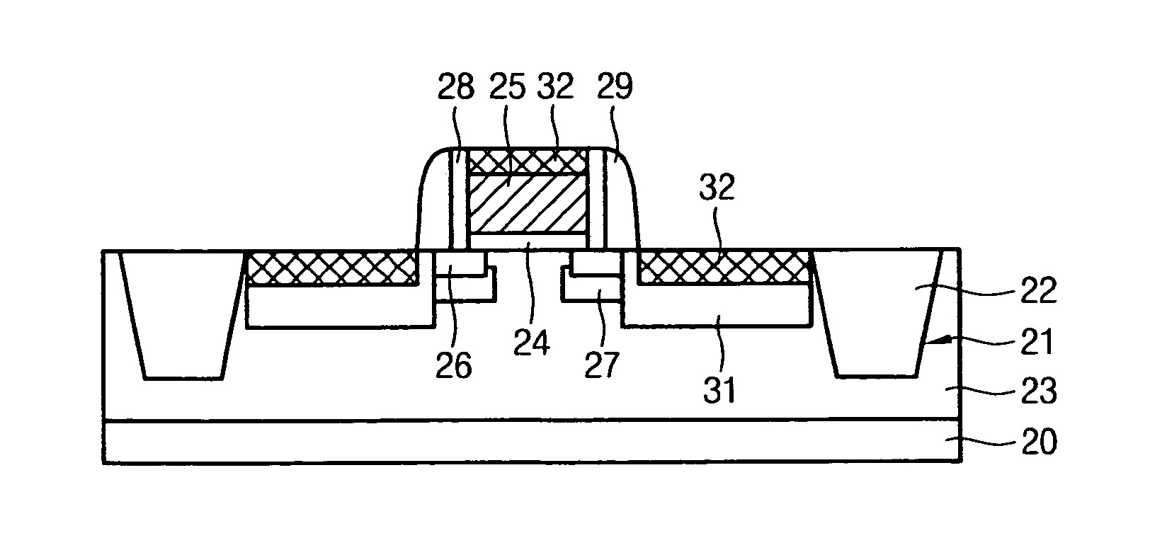
[0026]FIGS. 2A to 2G are sectional views for explaining a method of fabricating a transistor of a semiconductor device, with a PMOS FET as an example, according to one embodiment of the present invention.

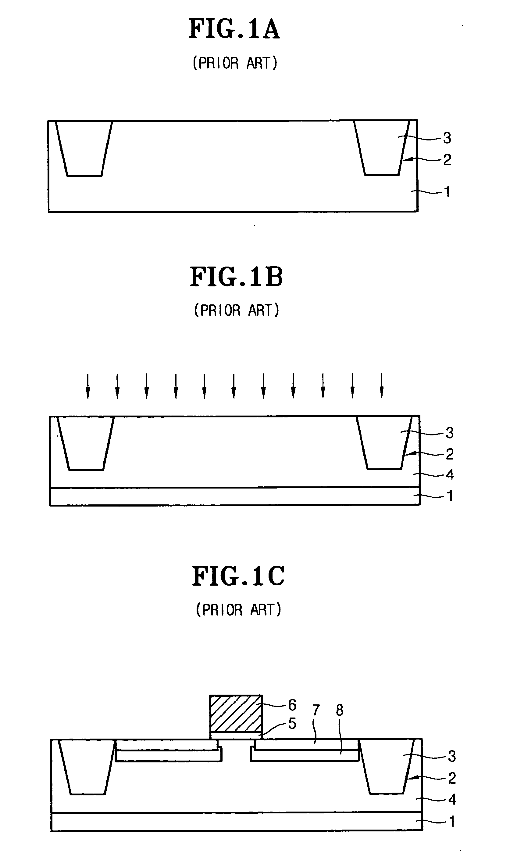
[0027] According to a method of fabricating a transistor of a semiconductor device according to the present invention, as shown in FIG. 2A, first, a semiconductor substrate 20 is provided in which the semiconductor substrate 20 has been divided into an active region (not shown) of the device and an isolation region (not shown). Subsequently, a shallow trench isolation (STI) process well-known in the art is performed to form an isolation layer 2...


PUM


Abstract

Disclosed is a method for fabricating a transistor of a semiconductor device, the method comprising the steps of: providing a semiconductor; forming a gate electrode; performing a low-density ion implantation process with respect to the substrate, thereby forming an LDD ion implantation layer; forming an insulation spacer on a sidewall of the gate electrode; forming a diffusion barrier; performing a high-density ion implantation process with respect to the substrate, thereby forming a source / drain; performing a first thermal treatment process with respect to a resultant structure, so as to activate impurities in the source / drain, and simultaneously causing a diffusion velocity of the impurities in the source / drain to be reduced by the diffusion barrier; and forming a salicide layer.

Description

BACKGROUND OF THE INVENTION [0001] 1. Field of the Invention [0002] The present invention relates to a method for fabricating a semiconductor device, and more particularly to a method for fabricating a transistor of a semiconductor device, which can improve a short channel effect by reducing a diffusion velocity of boron ions in a PMOS device. [0003] 2. Description of the Prior Art [0004] Recently, multimedia systems capable of simultaneously representing image, voice, character, etc., have been required to be fabricated with a compact size and a light weight, while being equipped with various kinds of complicated and advanced functions. In order to satisfy this demand, one-chip technology, which integrates semiconductor circuits having mutually different functions on the same chip so as to form one system, has been studied and developed. [0005] In a semiconductor circuit integrated on one chip, a plurality of circuits having different functions and operating at different voltages f...

Claims


Application Information

Patent Timeline
Patent Type & Authority Applications(United States)
IPC IPC(8): H01L21/265H01L21/336H01L21/335
CPCH01L21/26506H01L29/6659H01L29/665H01L21/26586H01L21/18
Inventor SA, SEUNG HOON
Owner ATRIA TECH INC
Why Eureka
Try Eureka