High voltage resistant edge structure for semiconductor components

a technology of semiconductor components and edge structures, applied in the direction of semiconductor devices, electrical appliances, basic electric elements, etc., can solve the problems of occupying a large amount of space in the design of this edge structure, consuming a great deal of space, and likewise consuming space in the realization of magnetoresistive rings in the edge region of semiconductor components

Inactive Publication Date: 2005-03-22
INFINEON TECH AG
View PDF24 Cites 75 Cited by
  • Summary
  • Abstract
  • Description
  • Claims
  • Application Information

AI Technical Summary

Benefits of technology

Proceeding on the basis of this prior art, it is the object of the present invention to set forth a simple and space-efficient embodiment...

Problems solved by technology

This edge structure consumes a great deal of space, accordingly.
The realization of these magnetoresistive rings in the edge region of the semiconductor component ...

Method used


Image

  • High voltage resistant edge structure for semiconductor components
  • High voltage resistant edge structure for semiconductor components
  • High voltage resistant edge structure for semiconductor components

Examples


Embodiment Construction

To the extent that they are not referenced otherwise, elements that are the same or that have the same function are provided with the same reference characters in all Figures of the drawing.

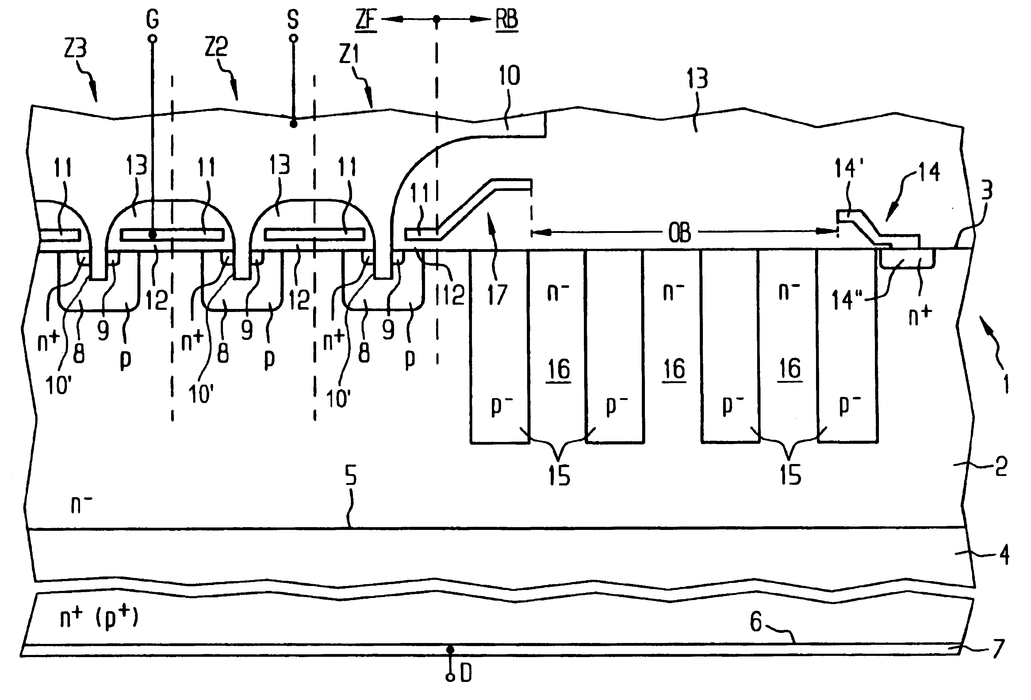
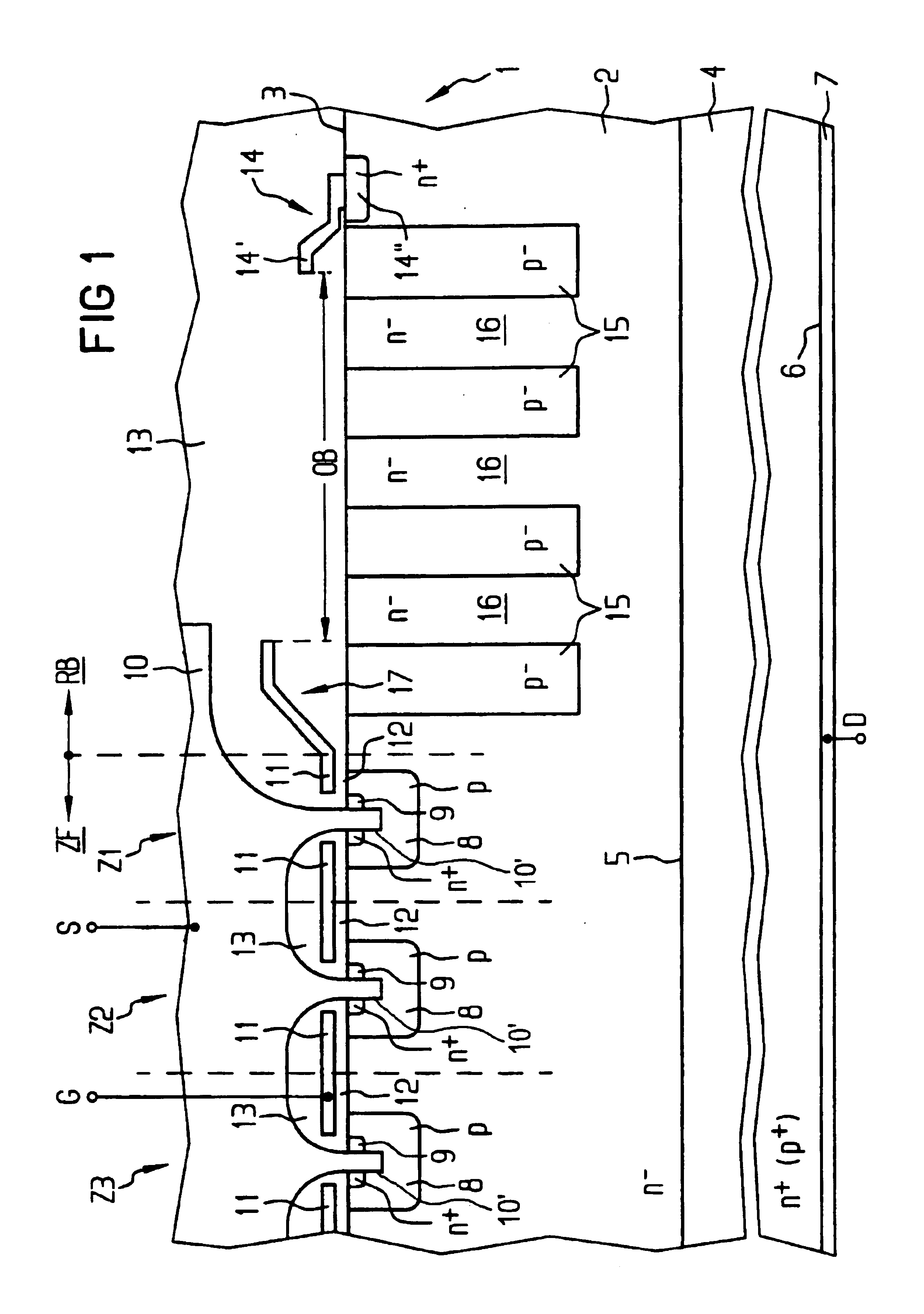
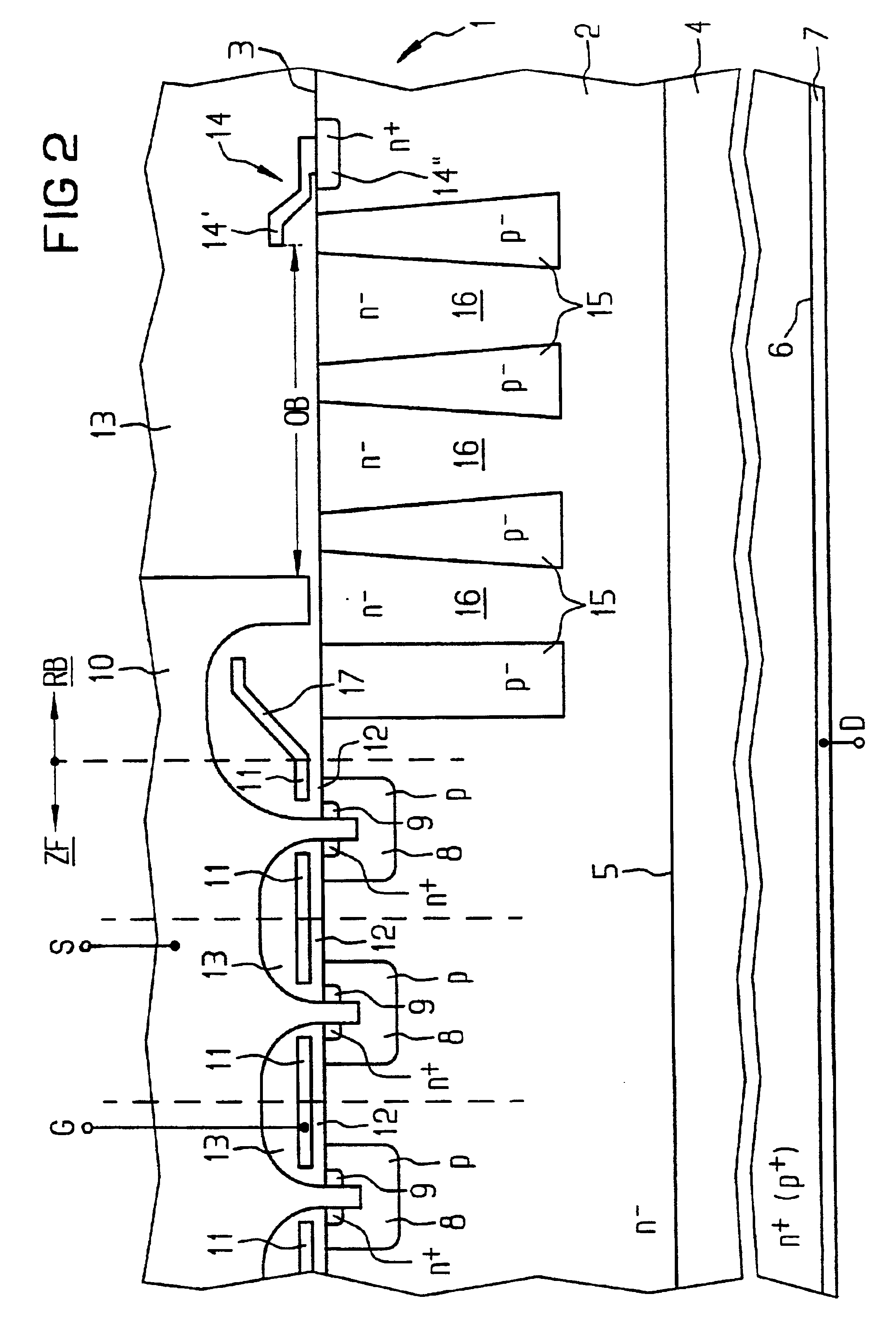
FIG. 1 shows a cross-section of a high voltage resistant (power) semiconductor component comprising an inventive edge structure.

The semiconductor component comprises a cell field ZF having a number of individual components, which are connected in parallel and are arranged in individual cells Z1 . . . Z3, of which the outermost three cells Z1 . . . Z3 are represented as cutouts only. The cell field ZF is terminated by an edge structure that is provided in the edge region RB of the semiconductor component. The edge region RB refers to the region of the semiconductor component located outside its active cells Z1 . . . Z3 of the cell field ZF.

In FIG. 1, the semiconductor body of the semiconductor component is referenced 1. The semiconductor body 1, which consists of silicon substrate, for example, co...


PUM


Abstract

The invention relates to a high voltage resistant edge structure in the edge region of a semiconductor component which has floating guard rings of the first conductivity type and inter-ring zones of the second conductivity type which are arranged between the floating guard rings, wherein the conductivities and/or the inter-ring zones are set such that their charge carriers are totally depleted when blocking voltage is applied. The inventive edge structure achieves a modulation of the electrical field both at the surface and in the volume of the semiconductor body. If the inventive edge structure is suitably dimensioned, the field intensity maximum can easily be situated in the depth; that is, in the region of the vertical p-n junction. Thus, a suitable edge construction which permits a “soft” leakage of the electrical field in the volume can always be provided over a wide range of concentrations of p and n doping.

Description

BACKGROUND OF THE INVENTIONThe present invention relates to a high voltage resistant edge structure in the edge region of a semiconductor component.Accordingly, a high voltage resistant edge structure in the edge region of a semiconductor component is provided, which has a semiconductor body, at whose first surface at least one inner zone of a first conductivity type is adjacent, at least one floating guard ring arranged in the inner zone, and at least one inter-ring zone of a second conductivity type arranged between the floating guard rings.In semiconductor elements, particularly in high voltage resistant power semiconductor components, voltage breakthroughs preferably arise in their edge region outside the doping zones, since the electrical field intensity is especially great there due to the is curvature of the doping zones which is conditioned by the edge. To avoid such voltage breakthroughs, doping zones are arranged in rings about the semiconductor components. These annular d...

Claims


Application Information

Patent Timeline
IPC IPC(8): H01L29/02H01L29/06H01L29/66H01L29/739H01L29/78H01L29/417
CPCH01L29/0634H01L29/41766H01L29/7802H01L29/7396H01L29/7395H01L29/7811
Inventor DEBOY, GERALDTIHANYI, JENOESTRACK, HELMUTGASSEL, HELMUTSTENGL, JENS-PEERWEBER, HANS
Owner INFINEON TECH AG
Why Eureka
Try Eureka