
CMP apparatus and process sequence method

a technology of process sequence and apparatus, which is applied in the direction of grinding machine components, manufacturing tools, lapping machines, etc., can solve the problem of unnecessary additional process cycles

Active Publication Date: 2006-10-10
TAIWAN SEMICON MFG CO LTD
View PDF6 Cites 20 Cited by
  • Summary
  • Abstract
  • Description
  • Claims
  • Application Information

AI Technical Summary

Benefits of technology

The present invention is about a new and improved CMP apparatus that includes multiple polishing pads and an in-line metrology tool. The metrology tool is used to measure the thickness of a material layer being polished on each of successive wafers in a lot prior to the final polishing step, in order to precisely polish the layer to a desired target thickness at the final polishing step. This renders unnecessary an additional process cycle to polish the layer to the desired target thickness. The metrology tool can provide not only the final fine polish desired amount but also to feed backward the optimal polish condition for prior polished step or steps of successive wafers by adjusting process time, pressure, head / platen rotation speed and slurry flow. The technical effect of this invention is to improve the precision and efficiency of the CMP process.

Problems solved by technology

This renders unnecessary an additional process cycle to polish the layer on each wafer to the desired target thickness.

Method used


Image

  • CMP apparatus and process sequence method
  • CMP apparatus and process sequence method
  • CMP apparatus and process sequence method

Examples


Embodiment Construction

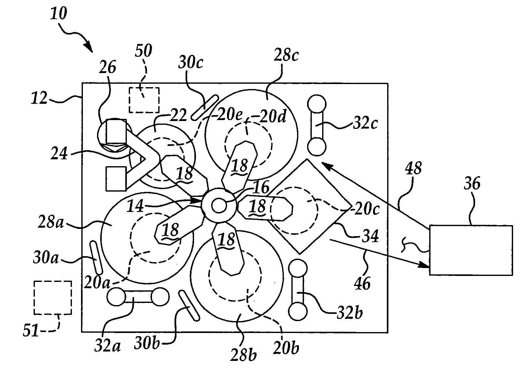
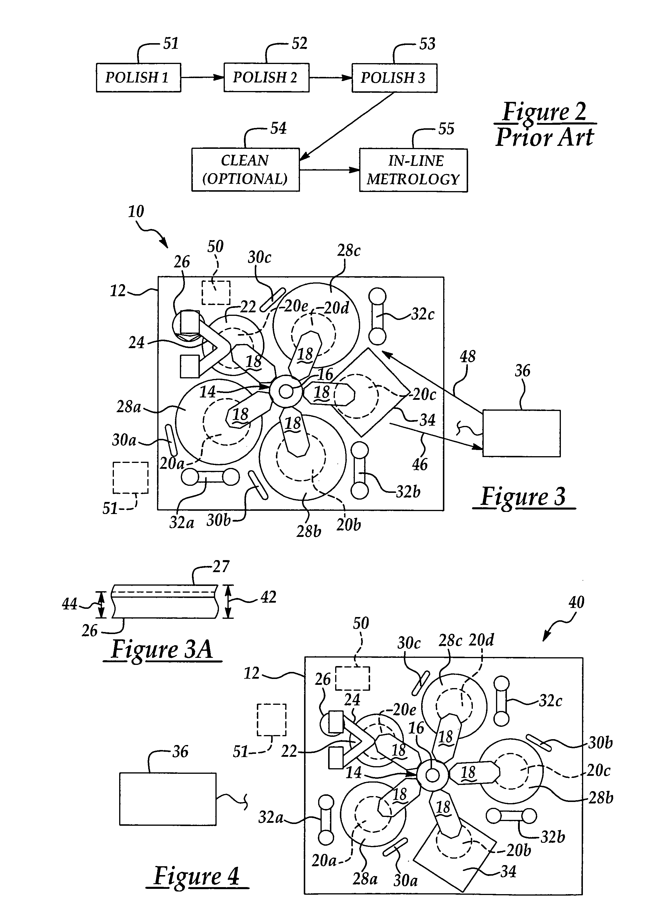
[0034]The present invention contemplates a new and improved CMP apparatus which includes multiple polishing pads and an in-line metrology tool which is interposed between adjacent polishing pads in the apparatus and may be modularized as a unit with the polishing pads. The CMP tool may include a base, multiple polishing pads provided on the base, a head rotation unit having multiple polishing heads provided above the polishing pads, a load / unload stage provided on the base for the loading and unloading of wafers to and from the polishing heads, and an in-line metrology tool interposed between two of the polishing pads on the base. The metrology tool is used to measure the thickness of a material layer being polished on each of successive wafers in a lot prior to the final polishing step or steps. This facilitates precise polishing of the layer to a desired target thickness at the final polishing step or steps and renders unnecessary an additional process cycle to polish the layer on...


PUM

PropertyMeasurementUnit
thicknessaaaaaaaaaa
thicknessaaaaaaaaaa
thicknessaaaaaaaaaa

Abstract

A CMP apparatus and process sequence. The CMP apparatus includes multiple polishing pads or belts and an in-line metrology tool which is interposed between adjacent polishing pads or belts in the apparatus. A material layer on each of multiple wafers is successively polished on the polishing pads or belts. The metrology tool is used to measure the thickness of a material layer being polished on each of successive wafers in a lot prior to the final polishing step, in order to precisely polish the layer to a desired target thickness at the final polishing step. This renders unnecessary an additional process cycle to polish the layer on each wafer to the desired target thickness. The metrology tool may be modularized as a unit with the polishing pads or belts.

Description

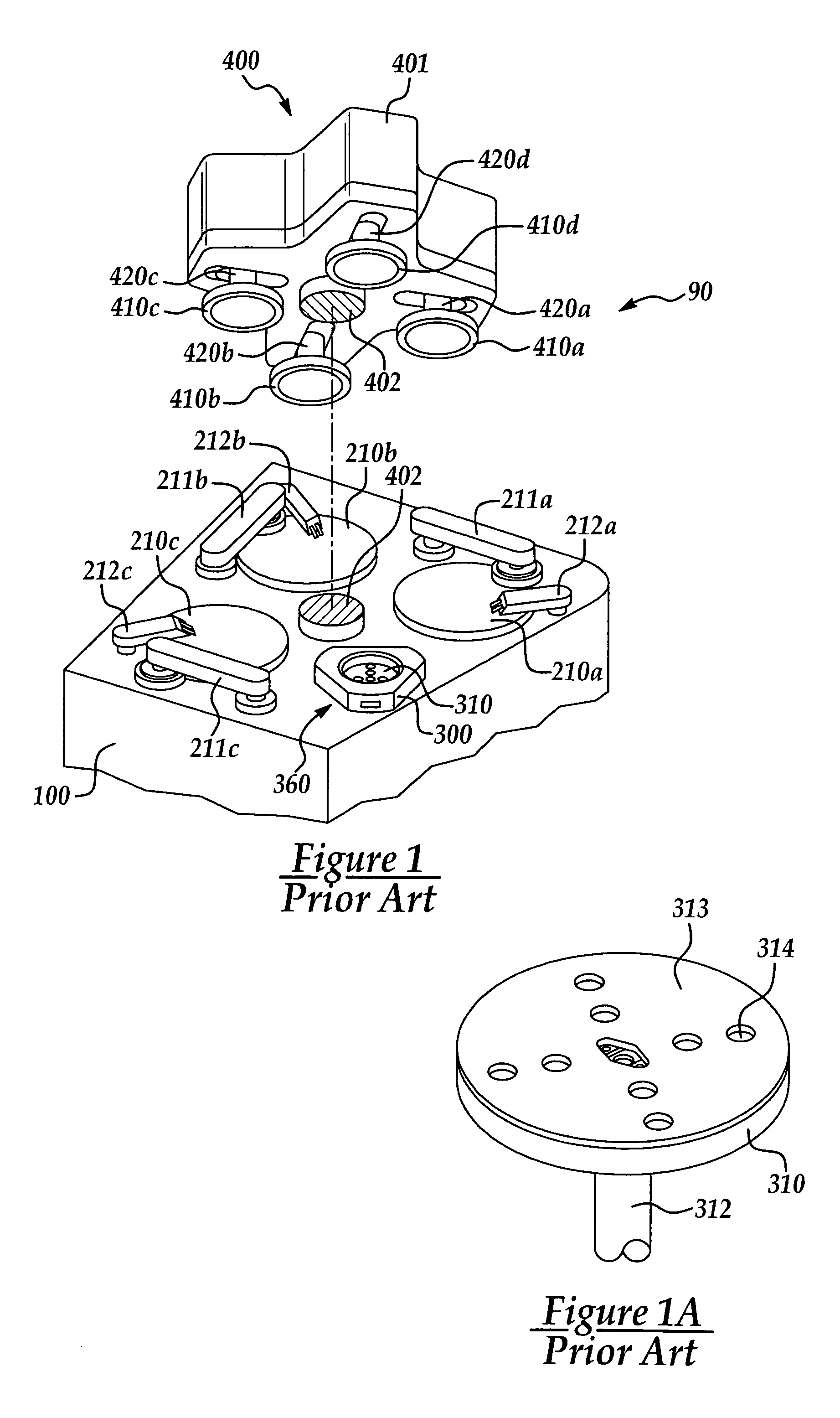
FIELD OF THE INVENTION[0001]The present invention relates to chemical mechanical polishing apparatus for polishing semiconductor wafer substrates. More particularly, the present invention relates to a new and improved CMP apparatus and process sequence method which includes the integration of CMP metrology between polishing steps to expedite polishing of multiple wafers.BACKGROUND OF THE INVENTION[0002]In the fabrication of semiconductor devices from a silicon wafer, a variety of semiconductor processing equipment and tools are utilized. One of these processing tools is used for polishing thin, flat semiconductor wafers to obtain a planarized surface. A planarized surface is highly desirable on a shallow trench isolation (STI) layer, inter-layer dielectric (ILD) or on an inter-metal dielectric (IMD) layer, which are frequently used in logic & memory devices. The planarization process is important since it enables the subsequent use of a high-resolution lithographic process to fabric...

Claims


Application Information

Patent Timeline
Patent Type & Authority Patents(United States)
IPC IPC(8): B24B49/00B24B1/00B24B7/22B24B21/04B24B37/04B24B49/02H01L21/304
CPCB24B21/04B24B49/02B24B37/345
Inventor CHEN, CHEN-SHIENHUANG, YAI-YEIKAO, MING-HSIANGLIN, YIH-SHUNGTJANDRA, WINATA KARTA
Owner TAIWAN SEMICON MFG CO LTD
Learn More