Memory module device for use in high-frequency operation

Active Publication Date: 2006-10-17
SAMSUNG ELECTRONICS CO LTD
View PDF4 Cites 20 Cited by
  • Summary
  • Abstract
  • Description
  • Claims
  • Application Information

AI Technical Summary

Benefits of technology

[0009]Another object of the present invention is to provide a memory module device capable of easily controlling a synchronization between data and a command address and easily obtaining a high frequency operation, and of reducing the number of command address pins.
[0012]A further additional object of the present invention is to provide a memory module device and a method therefor, which has an integrated buffer capable of reducing a propagation delay of a command address.
[0017]According to the configuration of the present invention, data signals and command address signals can be readily synchronized, and high frequency operation can be readily obtained.

Problems solved by technology

A memory system employing such a module has a problem in achieving greater than a 600 Mbps / pin data rate in the event that operating frequency is dictated by a 300 MHz dual edge clock, because of the “stub” connection configuration of the respective DQ buses.
Further, since a register and a buffer having each of process operations are independent of each other, it is difficult to achieve synchronization between the command address bus CA and the data bus DQ.

Method used


Image

  • Memory module device for use in high-frequency operation
  • Memory module device for use in high-frequency operation
  • Memory module device for use in high-frequency operation

Examples


third embodiment

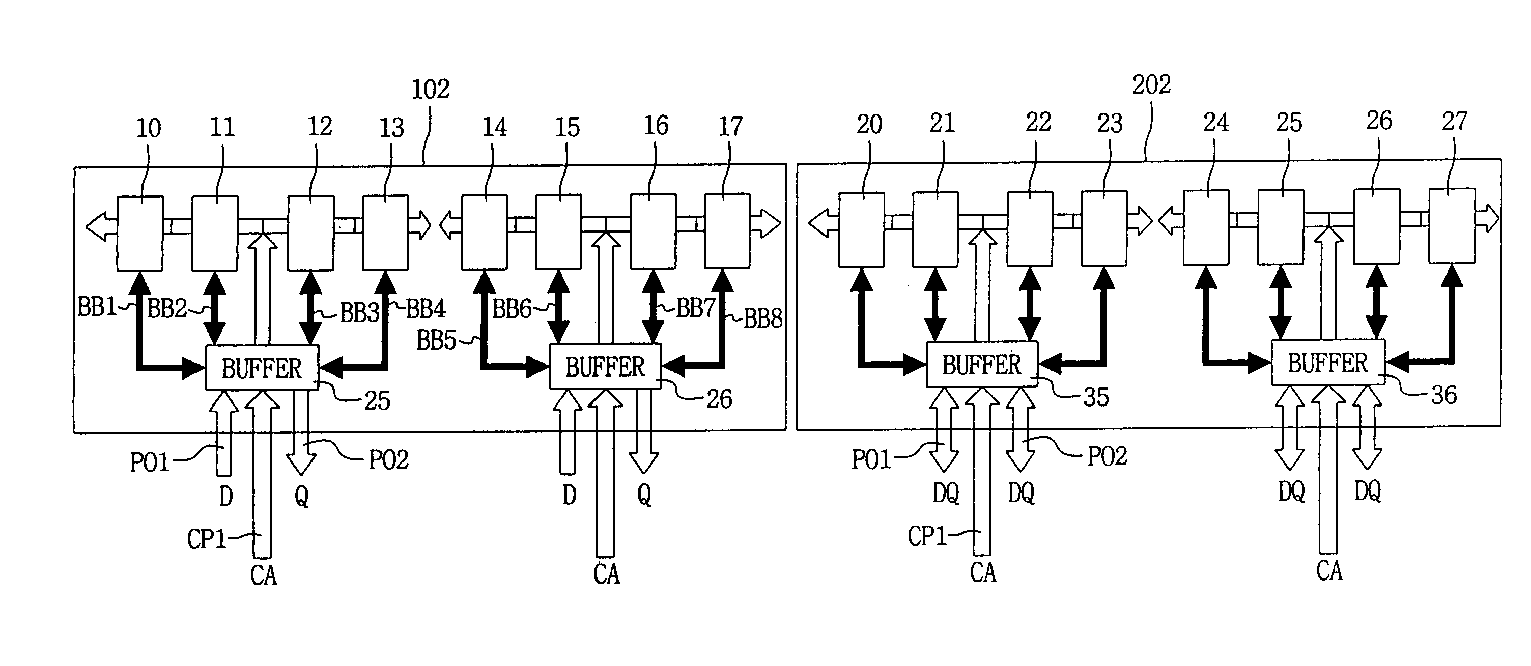
[0028]FIG. 5 is a block diagram illustrating the present invention. In the structure of FIG. 5, the CA register and the DQ buffer are once again integrated into a single chip 25A, 26A, 35a, 36a, as in the structure of FIG. 4, and further, all DQ buses and CA buses have the “point-to-point” bus structure. Therefore, since the CA signals and the DQ signals are synchronized in the memory system, the integrated buffer becomes released from the operation of synchronizing the CA and the DQ. Moreover, the CA and the DQ are simultaneously driven toward the DRAM from a single integrated chip, thus the CA and the DQ are synchronized easily at the DRAM. Also, as in the configuration of FIG. 4, the number of DRAMs driven by one integrated buffer is reduced to half, thus the propagation delay tPD of the CA signal is reduced to a half in comparison with the configuration of FIG. 3. As a result, operating frequency is improved, as discussed above. In this case, further, the frequency of the CA sig...


PUM


Abstract

A memory module device for use in a high frequency operation provides for ease in synchronization. In one example, the memory module includes integrated buffers, each having first and second data ports connected to respective data buses in a point-to-point configuration, such that data input through either data port of the first and second data ports is transferred to the memory device and is simultaneously output through the other data port of the first and second data ports. The integrated buffers each further include first and second command address ports connected to respective command address buses in a point-to-point configuration, such that a command address signal input through either port of the first and second command address ports is transferred to the memory device and simultaneously output through the other command address port of the first and second command address ports.

Description

BACKGROUND OF THE INVENTION[0001]1. Field of the Invention[0002]The present invention relates to a configuration of a high frequency DRAM module, and more particularly to a memory module device for use in a high-frequency operation.[0003]2. Description of the Related Art[0004]In electronic data processing (EDP) systems such as a personal computer (PC), a work station, a server etc., a memory device that is a main memory is commonly configured in a module in which a plurality of DRAMs are connected with one another via a system bus. To increase the overall efficiency of the EDP system, data transfer between the memory module and a system chip set, for example a CPU etc., must occur at a higher speed.[0005]Referring first to FIG. 1, which illustrates a block diagram of a conventional DRAM module, each of bilateral data buses (hereinafter, referred to as “DQ bus”) is connected directly to each of plural DRAMs 10–17 through a connector, and a command-address bus (hereinafter, referred t...

Claims


Application Information

Patent Timeline
IPC IPC(8): G06F12/00G11C7/10G11C5/02G11C11/4093
CPCG11C7/1051G11C7/1057G11C7/1078G11C7/1084G11C11/4093G11C5/02
Inventor KYUNG, KYE-HYUN
Owner SAMSUNG ELECTRONICS CO LTD
Why Eureka
Try Eureka