Nonvolatile semiconductor memory device and a method of the same

a nonvolatile semiconductor and memory device technology, applied in the direction of digital storage, solid-state devices, instruments, etc., can solve the problems of inability to produce floating gates having a desired shape with a good yield, short interval between any two adjacent selector gates therein, gate forming, etc., to promote the shrinkage of a nonvolatile semiconductor and increase the capacity of the same

Active Publication Date: 2006-10-24
RENESAS ELECTRONICS CORP
View PDF5 Cites 0 Cited by
  • Summary
  • Abstract
  • Description
  • Claims
  • Application Information

AI Technical Summary

Benefits of technology

[0013]An object of the present invention is to provide a technique for making the memory capacity of a nonvolatile semiconductor for a memory device large by promoting the shrinkage of its memory cells.
[0025]Briefly, an advantageous effect of the typical aspect of the present invention makes it possible to promote the shrinkage of a nonvolatile semiconductor for a memory device and to achieve an increase in the capacity thereof.

Problems solved by technology

However, in the case where the shrinkage of memory cells is further advanced, the interval between any two adjacent selector gates therein becomes very short according to the floating gate forming method described above.
Accordingly, it is difficult to deposit a polycrystal silicon film on a semiconductor substrate in such a way that selector gates are formed and, subsequently, a gap between any two adjacent ones out of these selector gates is buried with an antireflective film on the polycrystal silicon film inside the gap.
Therefore, it is impossible to produce floating gates having a desired shape with a good yield.

Method used


Image

  • Nonvolatile semiconductor memory device and a method of the same
  • Nonvolatile semiconductor memory device and a method of the same
  • Nonvolatile semiconductor memory device and a method of the same

Examples


embodiment 1

(Embodiment 1)

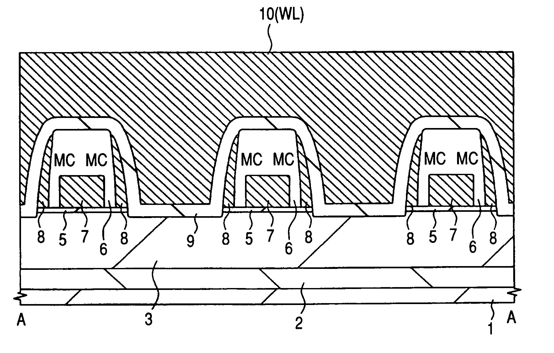
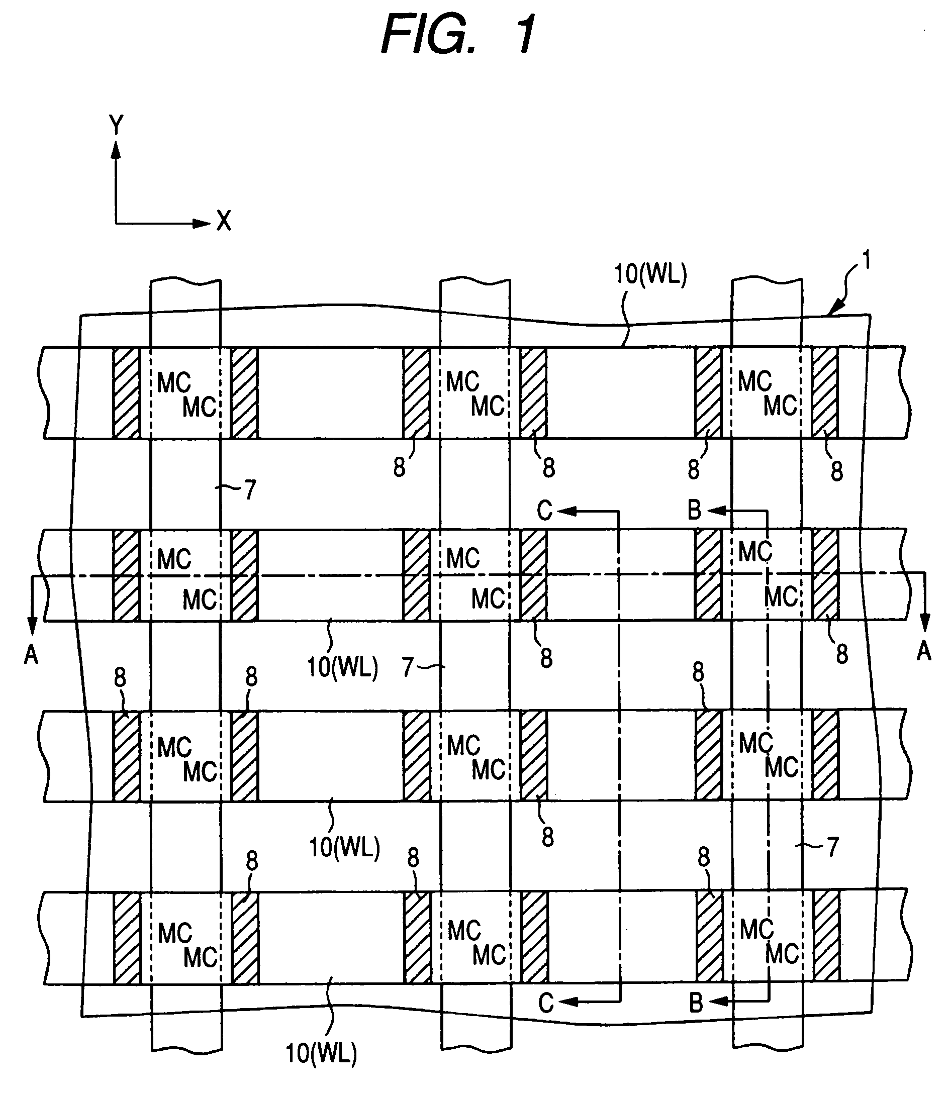
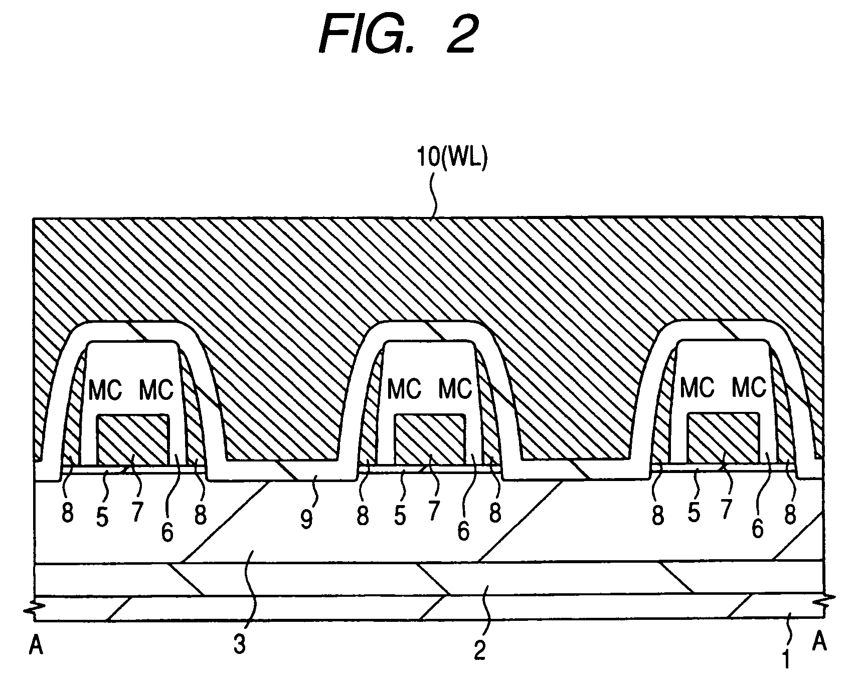
[0051]FIG. 1 is a partial plan view illustrating a memory mat structure of a flash memory which represents embodiment 1 of the present invention, FIG. 2 is a partial sectional view of a semiconductor substrate, which is taken along line A—A in FIG. 1, FIG. 3 is a partial sectional view of the semiconductor substrate, which is taken along line B—B in FIG. 1, and FIG. 4 is a partial sectional view of the semiconductor substrate, which is taken along line C—C in FIG. 1. In FIG. 1 (of the plane view), illustration of some members is omitted in order to make the pattern of an electroconductive layer easy to see.

[0052]The flash memory of the present embodiment is an AND mode flash memory having a capacity of 16 Gb (gigabits). Memory cells MC which constitute this flash memory are arranged, into a matrix form, in memory mat areas of a main surface of a semiconductor substrate 1, which will be referred to hereinafter merely as the substrate 1. The substrate 1 is made of a p-ty...

embodiment 2

(Embodiment 2)

[0091]FIG. 18 is a partial sectional view illustrating a memory mat area of a flash memory which represents embodiment 2 of the present invention.

[0092]As illustrated in FIG. 18, in each of the memory cells MC of the present embodiment, an n-type diffusion layer 4, functioning as a source and a drain, is formed in the surface of the p-type well 3 under each of the selector gates 7. This layer 4 is used as a bit line. This n-type diffusion layer 4 is formed under one of the side walls of the selector gate 7. In order to form the n-type diffusion layer 4, the selector gate 7 is formed over the p-type well 3 by the method illustrated in FIG. 14, and then oblique ion implantation is used to introduce an n-type impurity into the surface of the p-type well 3, as shown in FIG. 19.

[0093]As described above, in the flash memory of embodiment 1, at the time of applying a positive voltage to a selected one of the selector gates 7, the n-type reversion layer 11 formed on the surfac...


PUM


Abstract

A reduction in size nonvolatile semiconductors for use in a memory device and an increase in the capacity thereof are promoted. Each memory cell of a flash memory is provided with a field effect transistor having a first gate insulator film formed on a p-type well, a selector gate which is formed on the first insulator film and has side faces and a top face covered with a silicon oxide film (first insular film), floating gates which are formed in a side-wall form on both sides of the selector gate and which are electrically isolated from the selector gate through the silicon oxide film, a second gate insulator film formed to cover the silicon oxide film and the surface of each of the floating gates, and a control gate formed over the second gate insulator film.

Description

CROSS-REFERENCE TO RELATED APPLICATION[0001]The present application claims priority from Japanese patent application No. 2004-169660, filed on Jun. 8, 2004, the content of which is hereby incorporated by reference into this application.BACKGROUND OF THE INVENTION[0002]The present invention relates in general to a nonvolatile semiconductor for use as a memory device and to a method for producing the same, and, in particular, to a technique which is useful for achieving an increase in the memory capacity of flash memories.[0003]As a memory wherein data can be erased at a time, among nonvolatile semiconductor memories wherein data can be electrically rewritten, the so-called flash memory is known. The flash memory has excellent portability and impact resistance, and data memorized therein can be electrically erased at a time. In recent years, therefore, the demand for the flash memory has been expanding rapidly as a memory device for use in small-sized portable information-processing i...

Claims


Application Information

Patent Timeline
Patent Type & Authority Patents(United States)
IPC IPC(8): H01L29/76H01L29/788H01L21/8238H01L21/8247G11C11/34G11C16/04H01L27/10H01L27/115H01L29/423H01L29/792
CPCH01L27/115H01L27/11521H01L29/42328H01L29/7887G11C16/0458H10B69/00H10B41/30H01L29/66825
Inventor HARAGUCHI, KEIICHIKATO, MASATAKAKANAMITSU, KENJI
Owner RENESAS ELECTRONICS CORP
Why Eureka
Try Eureka