Method for entering circuit test mode

Inactive Publication Date: 2006-10-24
MONTEREY RES LLC
View PDF8 Cites 63 Cited by
  • Summary
  • Abstract
  • Description
  • Claims
  • Application Information

AI Technical Summary

Benefits of technology

[0008]The present invention provides for a method for entering test mode without adding to the pin count. Furthermore, embodiments provide for a method for entering test mode while minimizing the chance of accidentally entering test mode. Furthermore, embodiments provide for such a method which does not require complex circuitry to enter circuit test mode. The present invention provides these advantages and others not specifically mentioned above but described in the sections to follow.

Problems solved by technology

Testing a relatively complex circuit presents a number of challenges and trade-offs with respect to the use of the circuit's external pins.
While this simplifies the design, the pin count and hence the cost must be raised, if functionality is not to be sacrificed.
The fewer pins that the circuit has, the greater the problem of dedicating pins to testing becomes.
Testing circuits presents other problems as well, such as inadvertently entering test mode while the circuit is in its normal mode.
While this method may allow a pin to be used for more than just testing, this method is susceptible to noise accidentally causing entry to the test mode.
The result may be a program error requiring the user to reboot the computer.
Furthermore, the circuitry needed to support the above supervoltage technique may be complex.
Thus, the cost of the circuit may be increased.
Furthermore, the supervoltage circuitry may negatively impact issues such as circuit real estate and the designing of the circuit itself.
Still other problems are faced by the external testing device, which may have difficulty sending the analog waveform required by some circuits to put them into test mode.

Method used


Image

  • Method for entering circuit test mode
  • Method for entering circuit test mode
  • Method for entering circuit test mode

Examples


Embodiment Construction

[0020]In the following detailed description of the present invention, a method of entering circuit test mode, numerous specific details are set forth in order to provide a thorough understanding of the present invention. However, it will be recognized by one skilled in the art that the present invention may be practiced without these specific details or with equivalents thereof. In other instances, well known methods, procedures, components, and circuits have not been described in detail as not to unnecessarily obscure aspects of the present invention.

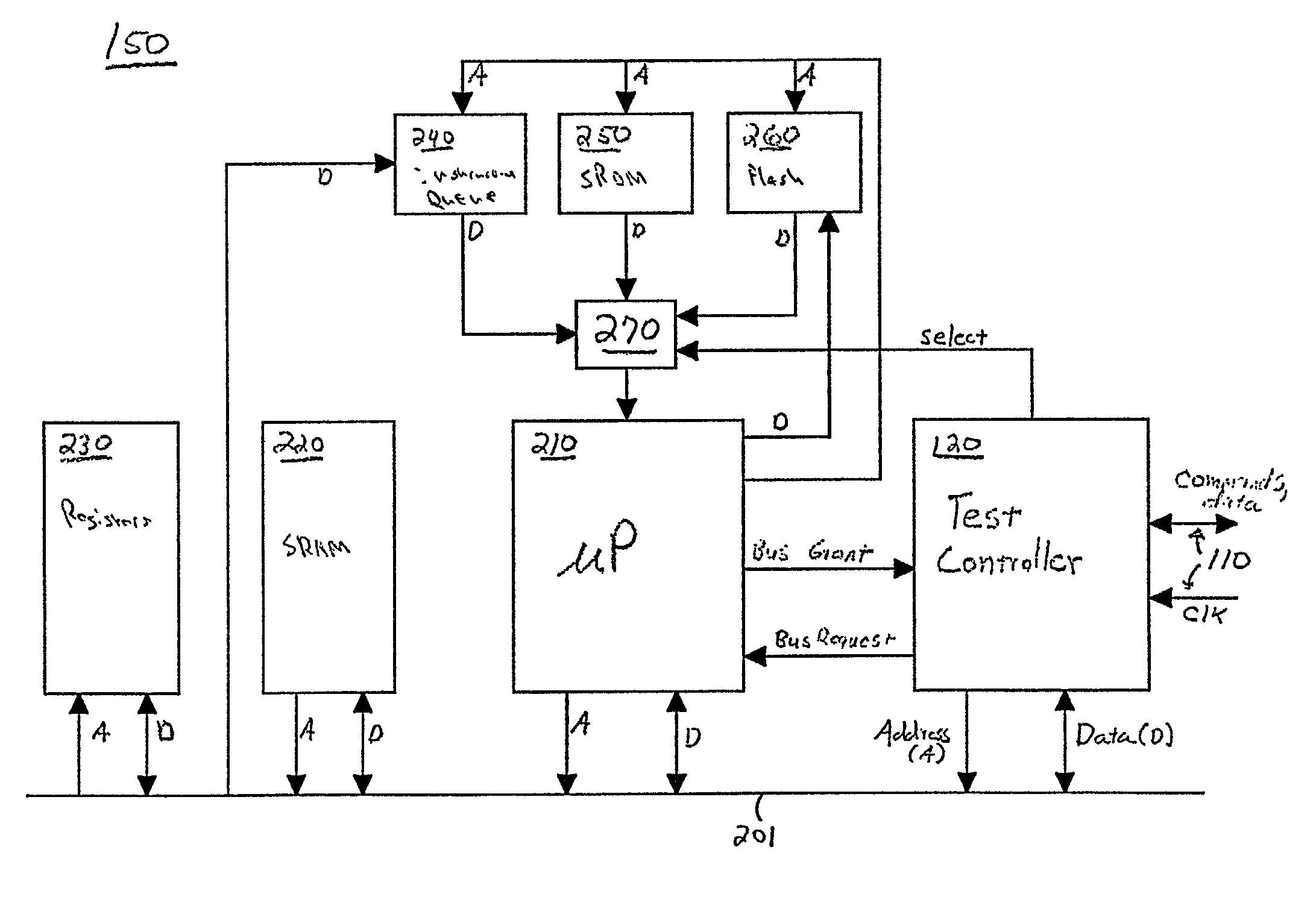
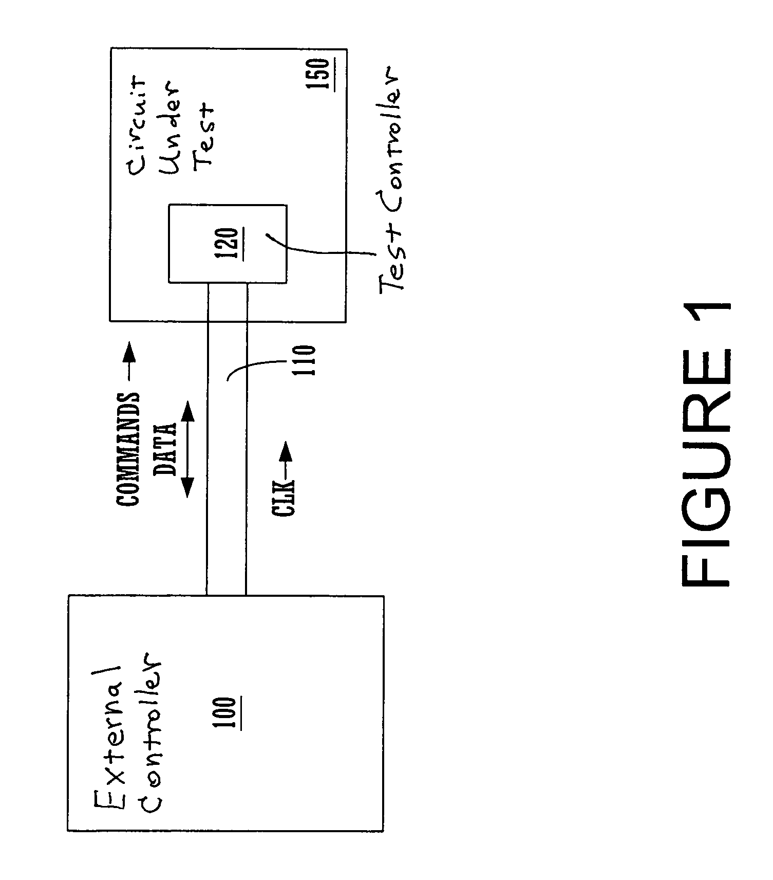
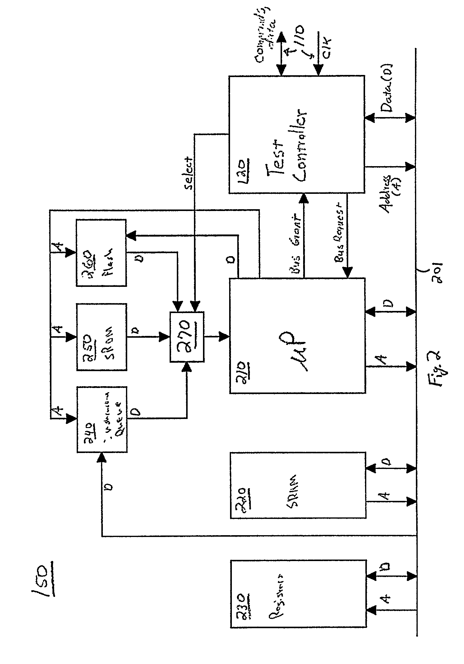
Exemplary Test Architecture

[0021]Embodiments of the present invention comprise a test architecture which includes an interface to a test controller located on the same bus as a microprocessor and various registers, memories, etc. under test. The test controller becomes the master during test mode and receives commands and data via the interface and sends data out the interface. The architecture features an instruction queue, which the ...


PUM


Abstract

A method for entering test mode of an integrated circuit device is disclosed. In one embodiment of the present invention, after a lockout period, a test controller generates a signal indicating the integrated circuit is willing to enter the test mode. After the signal, the test controller monitors a test interface during a predetermined period of time for a digital password. Then, in response to a valid password being received within the predetermined period, the test controller enters the test mode. In another embodiment, in addition to the above steps, in response to the valid password being received, the test controller generates an acknowledge signal. In one embodiment, the predetermined period of time takes place during a holdoff period after the lockout period. In another embodiment, the test interface is serial.

Description

RELATED U.S. APPLICATION[0001]This Application claims priority to the copending provisional patent application Ser. No. 60 / 243,708, entitled “ADVANCED PROGRAMMABLE MICROCONTROLLER DEVICE”, with filing date Oct. 26, 2000, and assigned to the assignee of the present application.FIELD OF THE INVENTION[0002]The present invention relates to the field of testing electronic circuitry. Specifically, the present invention relates to a method which provides entry into test mode without impacting chip performance.BACKGROUND ART[0003]Testing a relatively complex circuit presents a number of challenges and trade-offs with respect to the use of the circuit's external pins. As pins are a relatively expensive component of modern circuits, it is desirable to keep the pin count low. Some conventional architectures dedicate selected pins to testing the circuit. While this simplifies the design, the pin count and hence the cost must be raised, if functionality is not to be sacrificed. Alternatively, th...

Claims


Application Information

Patent Timeline
IPC IPC(8): G06F11/273G06F11/27G06F11/22
CPCG06F11/2236
Inventor SNYDER, WARREN
Owner MONTEREY RES LLC
Why Eureka
Try Eureka