Low power circuits for active matrix emissive displays and methods of operating the same

a low-power circuit and active matrix technology, applied in the field of active matrix emissive displays, can solve the problem of significant power consumption for producing light emissions, and achieve the effect of significant power savings and power savings

Inactive Publication Date: 2006-10-31
SILICONFILE TECH INC
View PDF72 Cites 30 Cited by
  • Summary
  • Abstract
  • Description
  • Claims
  • Application Information

AI Technical Summary

Benefits of technology

[0024]The embodiments described herein provide significant power savings by allowing a power TFT, that supplies currents to a light-emitting device such as an OLED in a pixel of a display, to operation in the unsaturated regions associated with its current-voltage characteristics, because the brightness of the light-emitting device according to embodiments of the present invention does not depend on a current-voltage relationship of the power TFT, but on the pixel brightness itself. Further power savings are achieved in embodiments using variable power supplies.

Problems solved by technology

The power problem in the AMLCD is typically in a backlight circuit that supplies the light, which the LCD modulates.
In the case of active matrix emissive displays, particularly the active matrix organic light emitting displays (AMOLED), significant amount of power is consumed to produce light emissions from the pixels, and additional power is required to operate driving circuits in the active matrix, which control the light emissions.
A problem arises because OLED D1 is a load on TFT T2, which load is changing during operation, as every level of luminance from OLED D1 requires a specific current ID, and thus, represents a different load to TFT T2.
Furthermore, even higher VD may be required to keep TFT T2 in saturation due to threshold voltage drift, which often happens with amorphous silicon TFTs.

Method used


Image

  • Low power circuits for active matrix emissive displays and methods of operating the same
  • Low power circuits for active matrix emissive displays and methods of operating the same
  • Low power circuits for active matrix emissive displays and methods of operating the same

Examples


Embodiment Construction

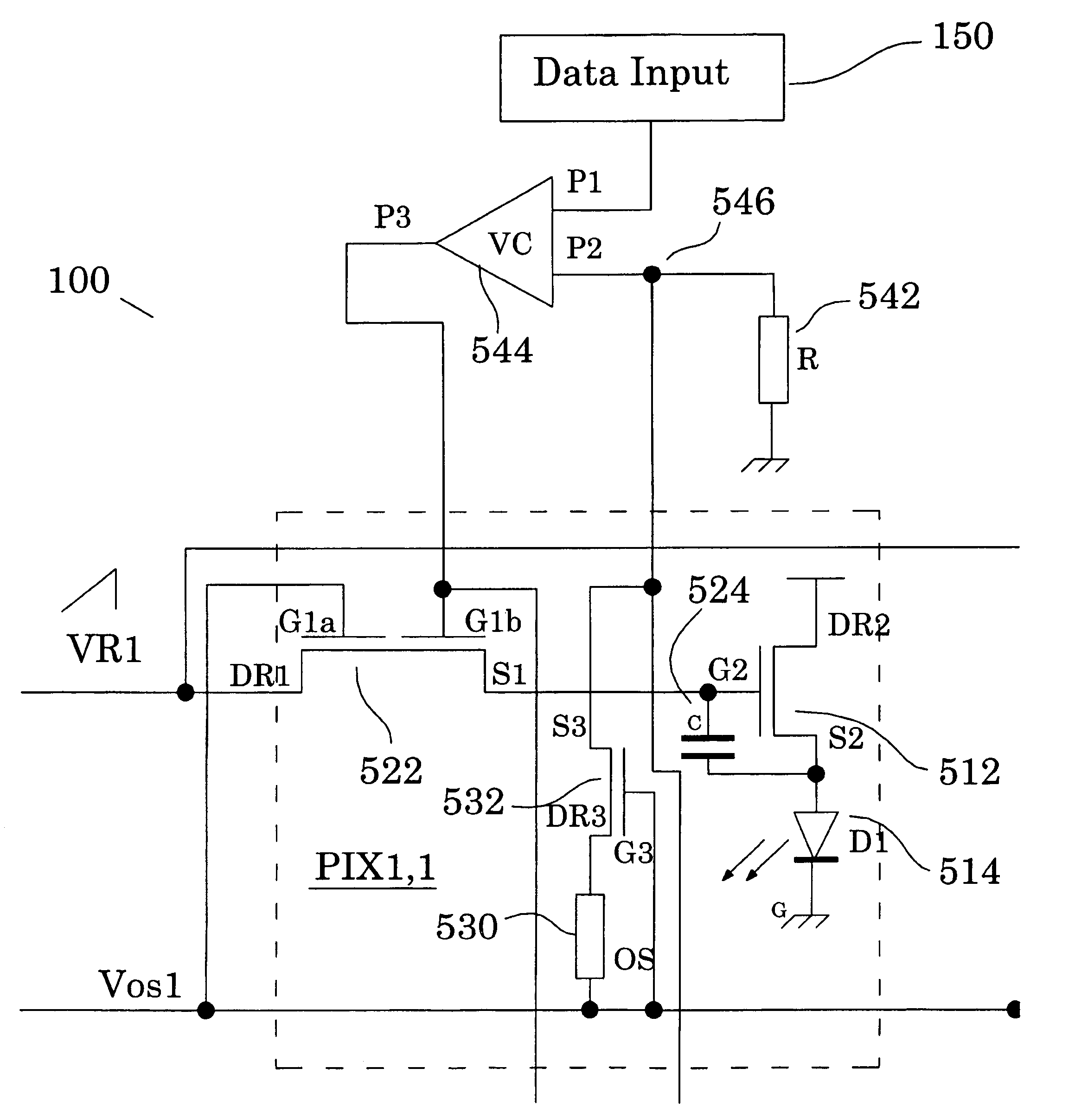
[0034]Embodiments of the present invention provide low-power circuits for emissive displays and methods of operating the same. The embodiments described herein save power consumed by power TFTs that supply currents to light-emitting devices in a display by allowing the power TFTs to operate in the unsaturated region.

[0035]FIG. 4A is a block diagram of a portion of an exemplary circuit 100 for a display, such as a flat panel display, according to one embodiment of the present invention. As shown in FIG. 4A, display circuit 100 comprises a light emission source 110, an emission driver 120 configured to vary the luminance of the emission source 110, an optical sensor 130 positioned to receive a portion of the light emitted from emission source 110 and having an associated electrical parameter dependent on the received light, a control unit 140 configured to control the driver 120 based on the changes in the electrical parameter of the sensor 130, and a data input unit 150 configured to...


PUM


Abstract

The embodiments of the present invention provide a flat panel display having a plurality of pixels, each comprising a light-emitting device configured to emit light in accordance with a current flowing through the light-emitting device, a transistor coupled to the light-emitting device and configured to provide the current through the light-emitting device, the current increasing with a ramp voltage applied to a control terminal of the transistor, and a switching device configured to switch off in response to the luminance of the light-emitting device having reached a specified level, thereby disconnecting the ramp voltage from the transistor and locking the brightness at the specified level. The switching device is further configured to stay off thereby allowing the luminance of the light-emitting device to be kept at the specified level until the pixel is rewritten in a different frame.

Description

CROSS REFERENCE TO RELATED APPLICATIONS[0001]The present application claims priority to U.S. Provisional Patent Application No. 60 / 561,474 entitled “Low Power Circuit for Active Matrix Emissive Flat Panel Displays,” filed on Apr. 12, 2004, the entire disclosure of which is incorporated herein by reference.[0002]The present application is related to commonly assigned U.S. patent application, entitled “Color Filter Integrated with Sensor Array for Flat Panel Display,” filed Apr. 6, 2005, commonly assigned U.S. patent application Ser. No. 10 / 872,344, entitled “Method and Apparatus for Controlling an Active Matrix Display,” filed Jun. 17, 2004, and commonly assigned U.S. patent application Ser. No. 10 / 841,198 entitled “Method and Apparatus for Controlling Pixel Emission,” filed May 6, 2004, each of which is incorporated herein by reference.FIELD OF THE INVENTION[0003]The present invention relates to active matrix emissive displays and particularly to low power circuits for active matrix...

Claims


Application Information

Patent Timeline
Patent Type & Authority Patents(United States)
IPC IPC(8): G09G5/00G09G3/30G09G3/32
CPCG09G3/3233G09G3/3266G09G3/3291G09G3/2011G09G2300/0814G09G2300/0819G09G2300/0842G09G2310/0259G09G2320/0209G09G2320/0285G09G2330/021G09G2330/028G09G2360/148
Inventor NAUGLER, JR., W. EDWARD
Owner SILICONFILE TECH INC
Why Eureka
Try Eureka