Supercharge Your Innovation With Domain-Expert AI Agents!

Integrated circuit with multi-length output transistor segment

a technology of integrated circuits and output transistors, which is applied in the direction of transistors, semiconductor devices, electrical equipment, etc., can solve the problems of ic circuitry that is often required for output transistors, adversely changing the electrical properties of ic circuitry, and fabricated on a semiconductor die having a very large or very small aspect ratio , to achieve the effect of reducing the number of transistors

Inactive Publication Date: 2006-11-14
POWER INTEGRATIONS INC
View PDF12 Cites 61 Cited by
  • Summary
  • Abstract
  • Description
  • Claims
  • Application Information

AI Technical Summary

Benefits of technology

This approach enhances area efficiency and reduces mechanical stress, enabling a range of current handling capabilities within a standardized package size, improving the overall performance and reliability of integrated circuits.

Problems solved by technology

An IC fabricated on a semiconductor die having a very large or very small aspect ratio often suffers from mechanical stress caused by the molding compound used to package the die.
This stress can adversely change the electrical properties of the IC circuitry.
The difficulty, however, is that the output transistors are often required to have elongated segments in order to achieve area efficiency and a specific current handling capability.
However, this causes area inefficiencies due to control circuit wiring.
Another significant shortcoming of this prior art approach is that in IC devices with small output field-effect transistors (i.e., fewer segments) suffer from package stress problems caused by high semiconductor die aspect ratio.
Thus, there is an unsatisfied need for an improved monolithic IC design that overcomes the problems of poor control circuit area efficiency and high IC aspect ratio.

Method used


Image

  • Integrated circuit with multi-length output transistor segment
  • Integrated circuit with multi-length output transistor segment
  • Integrated circuit with multi-length output transistor segment

Examples


Embodiment Construction

[0017]An improved integrated circuit is described. In the following description, numerous specific details are set forth, such as device types, dimensions, circuit configurations, etc., in order to provide a thorough understanding of the present invention. However, persons having ordinary skill in the semiconductor arts will appreciate that these specific details may not be needed to practice the present invention.

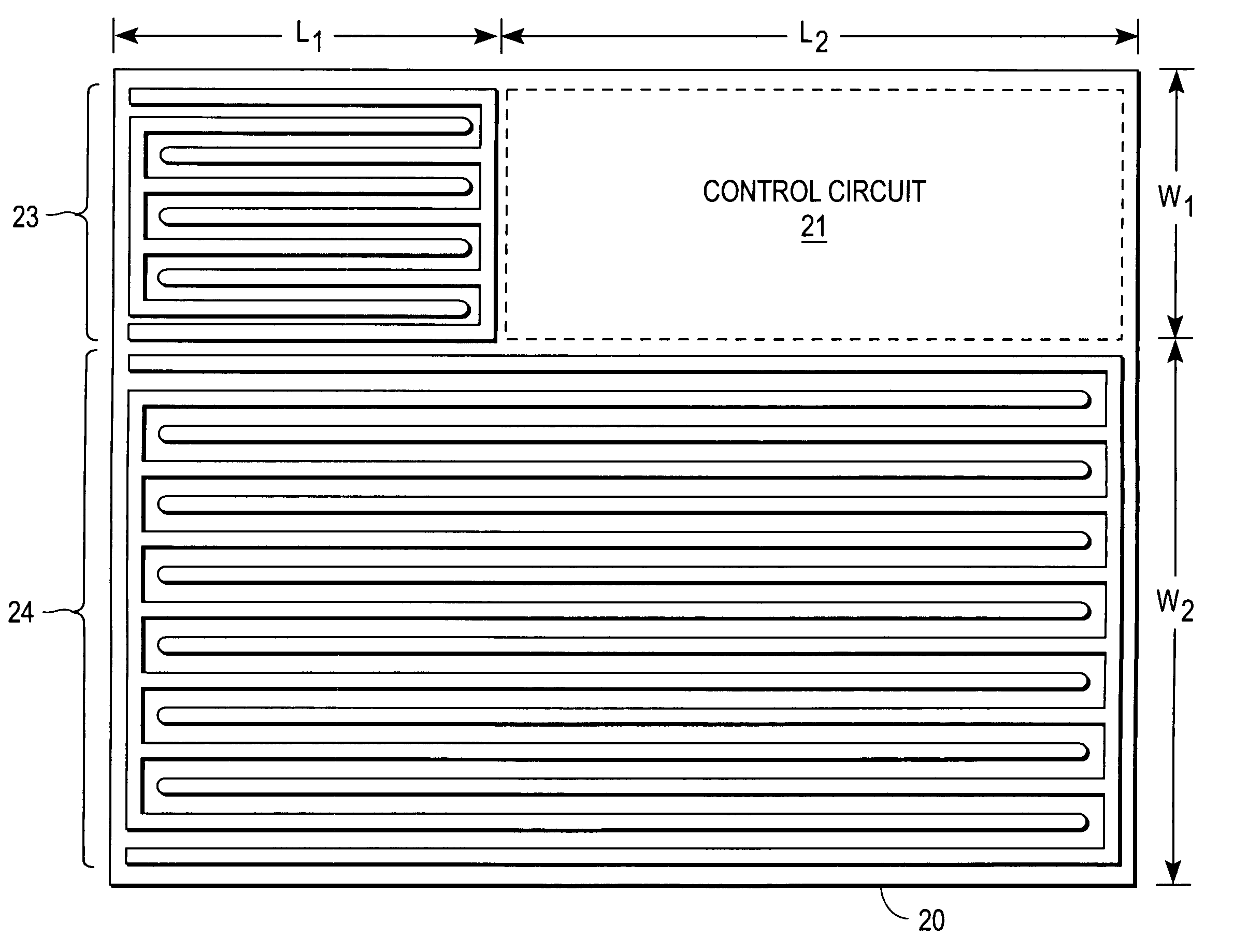
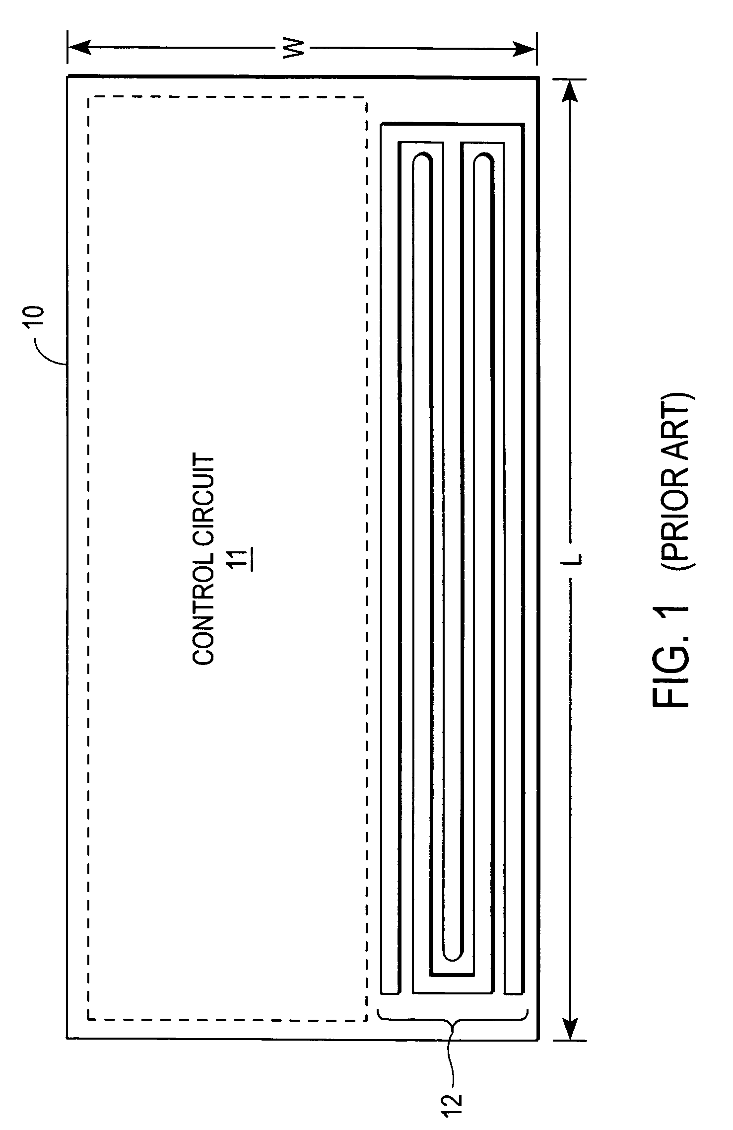
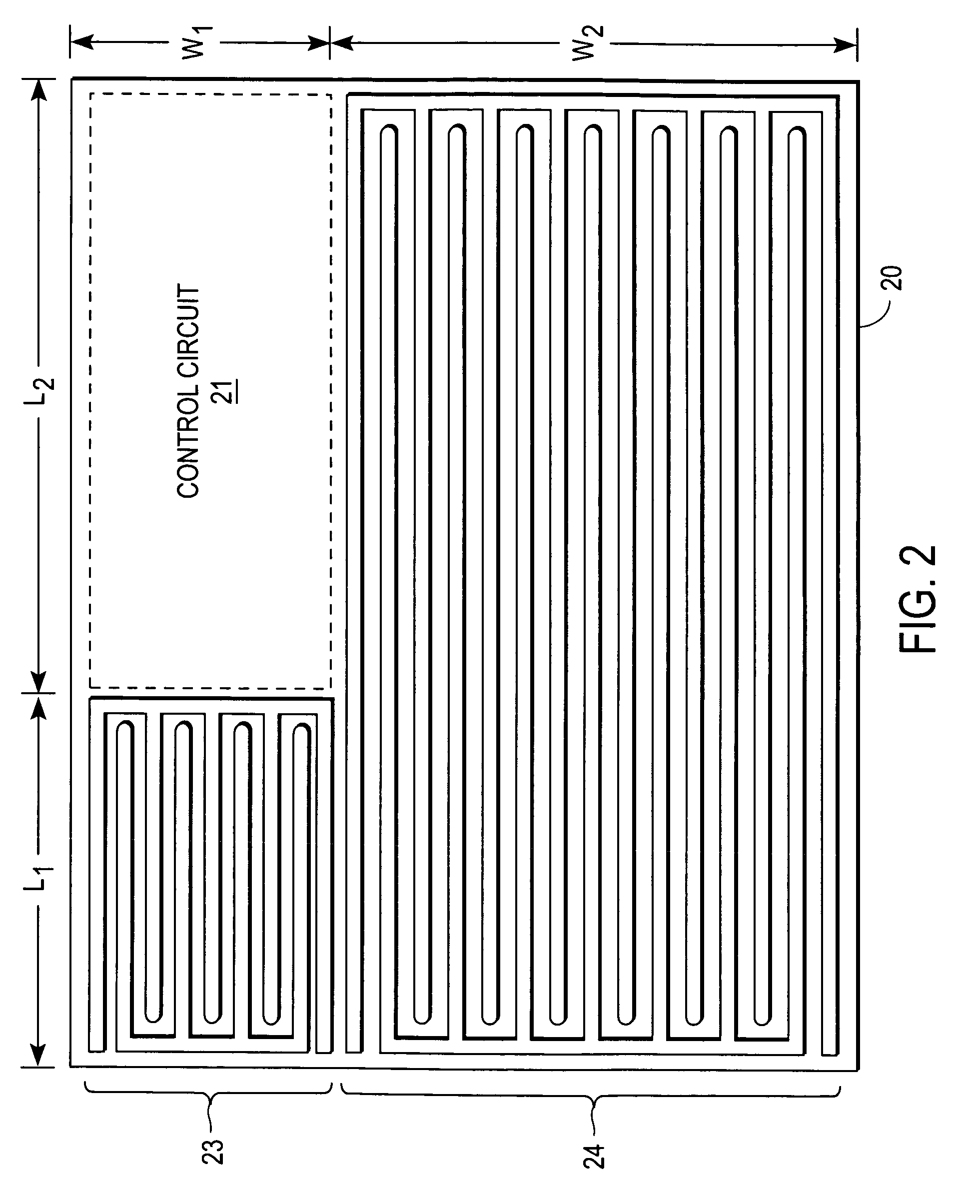
[0018]FIG. 2 illustrates a circuit layout of a monolithic IC according to one embodiment of the present invention. (In the context of the present application, the term “IC” is considered synonymous with a monolithic device.) In the example of FIG. 2, the IC shown may comprise a power integrated circuit (PIC) fabricated on a semiconductor die 20, which includes a first output HVFET 23 having a set of relatively short interdigitated source / drain segments, and a second output HVFET 24 having a set of relatively long interdigitated source / drain segments. The segments of HVFETs...


PUM


Abstract

A monolithic integrated circuit fabricated on a semiconductor die includes a control circuit and a first output transistor having segments substantially equal to a first length. A second output transistor has segments substantially equal to a second length. The first and second output transistors occupy an L-shaped area of the semiconductor die, the L-shaped area having first and second inner sides that are respectively disposed adjacent first and second sides of the control circuit. At least one of the first and second output transistors is coupled to the control circuit. It is emphasized that this abstract is provided to comply with the rules requiring an abstract that will allow a searcher or other reader to quickly ascertain the subject matter of the technical disclosure. It is submitted with the understanding that it will not be used to interpret or limit the scope or meaning of the claims. 37 CFR 1.72(b).

Description

RELATED APPLICATIONS[0001]This is a continuation-in-part (CIP) application of application Ser. No. 10 / 974,176 filed Oct. 26, 2004, entitled, “INTEGRATED CIRCUIT WITH MULTI-LENGTH POWER TRANSISTOR SEGMENTS”, which is assigned to the assignee of the present CIP application.FIELD OF THE INVENTION[0002]The present invention relates generally to the field of semiconductor devices; more specifically, to monolithic integrated circuits (ICs) and to methods of manufacturing IC devices.BACKGROUND OF THE INVENTION[0003]Integrated circuits (ICs), including power integrated circuits (PICs), find application in an increasingly wide variety of electronic devices. Typically, PICs comprise one or more high-voltage field effect transistors (HVFETs) having a device structure such as those disclosed in U.S. Pat. No. 6,207,994 (“the '994 patent”), which is herein incorporated by reference. Each of the devices disclosed in the '994 patent has a source region and a drain region separated by an intermediat...

Claims


Application Information

Patent Timeline
Patent Type & Authority Patents(United States)
IPC IPC(8): H01L29/772
CPCH01L27/0203H01L27/0207H01L27/088H01L29/41758H01L29/7835
Inventor BALAKRISHNAN, BALU
Owner POWER INTEGRATIONS INC
Features
  • R&D
  • Intellectual Property
  • Life Sciences
  • Materials
  • Tech Scout
  • Unparalleled Data Quality
  • Higher Quality Content
  • 60% Fewer Hallucinations
Learn More