Semiconductor device with guard ring for preventing water from entering circuit region from outside

Active Publication Date: 2006-11-21
RENESAS ELECTRONICS CORP
View PDF3 Cites 27 Cited by
  • Summary
  • Abstract
  • Description
  • Claims
  • Application Information

AI Technical Summary

Benefits of technology

[0006]It is therefore an object of the present invention to provide a semiconductor device whi

Problems solved by technology

When the semiconductor device is scri

Method used


Image

  • Semiconductor device with guard ring for preventing water from entering circuit region from outside
  • Semiconductor device with guard ring for preventing water from entering circuit region from outside
  • Semiconductor device with guard ring for preventing water from entering circuit region from outside

Examples


1st embodiment

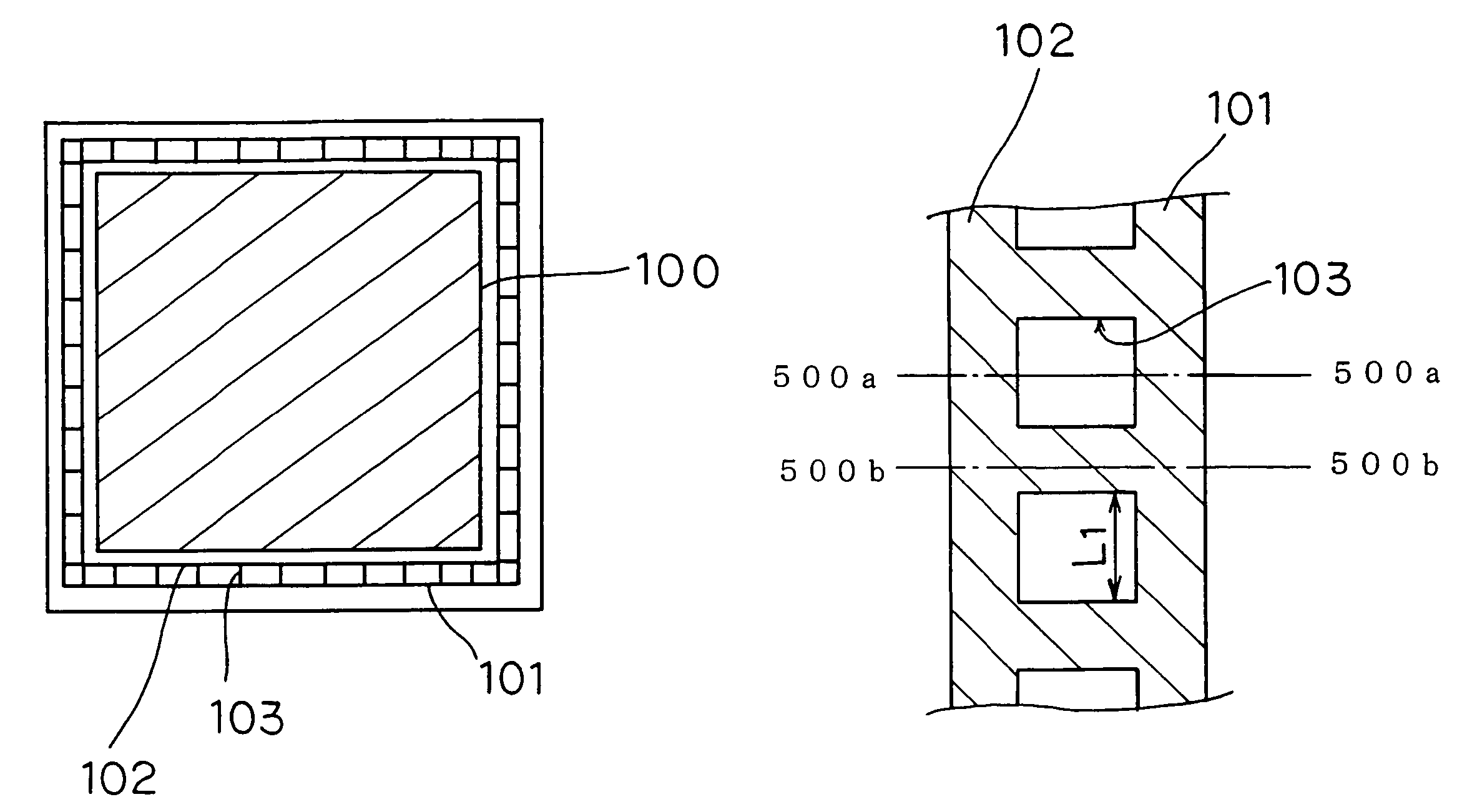
[0026]FIG. 1A shows in plan a semiconductor device according to a first embodiment of the present invention, and FIG. 1B shows in enlarged fragmentary plan a guard ring assembly of the semiconductor device according to the first embodiment.

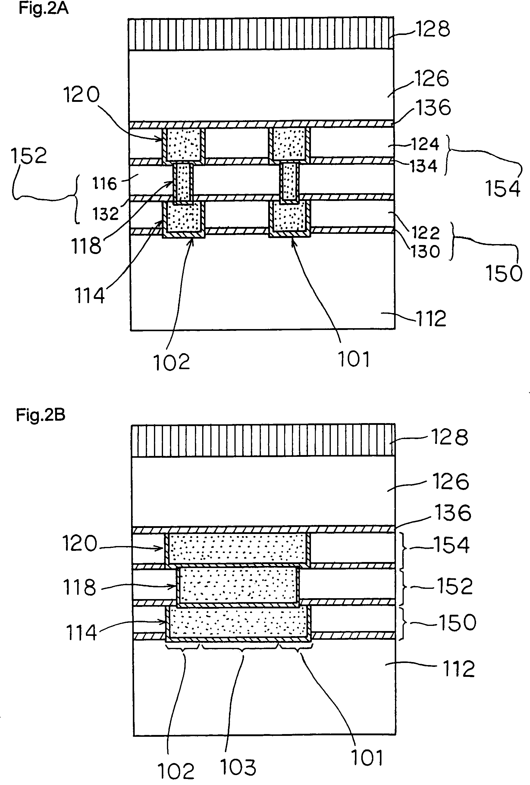
[0027]As shown in FIG. 1A, the semiconductor device according to the first embodiment comprises circuit region 100 circuits such as memories, logic circuits, etc., are formed, two guard rings 101, 102 extending along the periphery of the chip, and a plurality of connections 103 interconnecting two guard rings 101, 102. Guard ring 101 is disposed closely to the periphery of the chip, and guard ring 102 is disposed between guard ring 101 and circuit region 100.

[0028]As shown in FIG. 1B, two guard rings 101, 102 are interconnected by connections 103 that are spaced at predetermined intervals. Connections 103 divide the area sandwiched between two guard rings 101, 102 into a plurality of subareas. In FIG. 1B, two adjacent connections 103 are spaced fr...

2nd embodiment

[0061]A semiconductor device according to a second embodiment of the present invention has three or more guard rings.

[0062]Those parts of the semiconductor device according to the second embodiment which are identical to those of the semiconductor device according to the first embodiment are denoted by identical reference characters, and will not be described in detail below.

[0063]FIG. 7A shows in plan the semiconductor device according to the second embodiment of the present invention, and FIG. 7B shows in enlarged fragmentary plan guard rings of the semiconductor device according to the second embodiment.

[0064]As shown in FIG. 7A, the semiconductor device according to the second embodiment has guard ring 201 disposed between guard ring 102 and circuit region 100 of the semiconductor device according to the first embodiment, and hence has three guard rings. Guard rings 101, 102 are connected to each other by a plurality of connections 103a, and guard rings 102, 201 are connected to...

3rd embodiment

[0068]A semiconductor device according to a third embodiment of the present invention has three or more guard rings. The semiconductor device according to the third embodiment is similar to the semiconductor device according to the second embodiment except that the junctions between connections 103a and guard ring 102 and the junctions between connections 203 and guard ring 102 are positioned out of alignment with each other.

[0069]Those parts of the semiconductor device according to the third embodiment which are identical to those of the semiconductor devices according to the first and second embodiments are denoted by identical reference characters, and will not be described in detail below.

[0070]FIG. 8A shows in plan the semiconductor device according to the third embodiment of the present invention, and FIG. 8B shows in enlarged fragmentary plan guard rings of the semiconductor device according to the third embodiment.

[0071]As shown in FIG. 8A, guard ring 201 is disposed between...


PUM


Abstract

A semiconductor device has a first guard ring surrounding a circuit region, a second ring disposed between the circuit region and the first guard ring, and first connections connecting the first guard ring and the second guard ring to each other. An area sandwiched between the first guard ring and the second guard ring is divided by the first connections into a plurality of subareas. Even if the first guard ring is partly defective, water enters from outside into only the subarea which is contiguous to the defective part of the first guard ring.

Description

BACKGROUND OF THE INVENTION[0001]1.Field of the Invention[0002]The present invention relates to a semiconductor device having a circuit region where semiconductor components such as transistors or the like are formed.[0003]2.Description of the Related Art[0004]Heretofore, semiconductor devices have had a circuit region where circuits such as memories, logic circuits, etc., are formed, and a guard ring for preventing water from entering the circuit region from the surrounding area. The guard ring extends along the periphery of the chip and is made of a metal such as copper (Cu) or the like. One known guard ring is disclosed in Japanese Patent Laid-open Publication No. 45766 / 97,for example, as follows: A semiconductor device has an outer guard ring disposed near the periphery of a chip and an inner guard ring disposed between the outer guard ring and a circuit region. The outer guard ring and the inner guard ring jointly make up a double guard ring assembly. The double guard ring asse...

Claims


Application Information

Patent Timeline
IPC IPC(8): H01L29/00H01L23/52H01L21/02H01L21/3205H01L23/00H01L23/58H01L29/74
CPCH01L23/585H01L2924/0002H01L2924/00
Inventor TOMITA, RYUJIKUROKAWA, TETSUYAISHIGAMI, TAKASHIIGUCHI, MANABUUENO, KAZUYOSHISEKINE, MAKOTO
Owner RENESAS ELECTRONICS CORP
Why Eureka
Try Eureka