Intrinsic thermal enhancement for FBGA package

a technology of bga and fbga, applied in the field of semiconductor devices, can solve the problems of reducing the surface area essential for thermal heat transfer, increasing the size and complexity of semiconductor devices, and enhancing microchip cooling, so as to achieve the effect of conducting a relatively large amount of heat away, reducing junction temperature, and increasing the thermal performance of fbga and bga packages

Inactive Publication Date: 2006-11-21
MICRON TECH INC
View PDF26 Cites 33 Cited by
  • Summary
  • Abstract
  • Description
  • Claims
  • Application Information

AI Technical Summary

Benefits of technology

[0011]In a further embodiment, the semiconductor device comprises a semiconductor die disposed on a thermally conductive plane (heat sink) layer on one side of an insulative support substrate. Thermally conductive via interconnects extend through the insulative substrate to the heat sink layer. A conductive (signal) layer of electrically conductive traces overlies at least a portion of the second side of the insulative support substrate. A first array of electrically conductive ball contacts is disposed on bonding pads connected to the traces to provide signal interconnects between the die and an external device such as a mother board. In one embodiment, a second array of thermally conductive ball contacts that are not connected to signal traces (“dummy balls”) are mounted on the second side of the support substrate in contact with the via interconnects to provide thermal grounding for cooling the device. Heat from the die passes through the thermally conductive plane (heat sink) layer through the via interconnects and into the thermally conductive dummy balls to a mother board or other external device on which the semiconductor device is mounted. In another embodiment, the second (thermal) ball array is connected by ground traces to the first (signal) ball array. The ground trace connection provides a thermal path from the metal plane layer (heat sink) to the first array of ball contacts, and a signal path from the first ball array to the metal plane (ground) layer. The ground trace connection provides a nearer return path for the signal trace to return to the external system ground such as a mother board ground, via the ball contacts for better signal integration of the system, and improved signal performance and solder joint reliability performance.
[0016]The resulting combination of a thick (copper) plane layer as a heat sink or heat spreader, a thin insulative support substrate, and additional sets of thermally conductive interconnect vias contact balls in excess of the typical number of contact balls (e.g., 54 balls, etc.) required in a standard FBGA package provides enhanced thermal performance of FBGA and BGA packages by reducing the junction temperature without the use of extrinsically attached heat sinks and heat spreaders. The present semiconductor device achieves a reduction of the junction temperature (Tj) up to about 10° C. compared to a package made with a single layer of copper traces on the underside of an insulative core substrate (e.g., FIG. 12) with no intrinsic heat sink layer interfacing with the die, and no thermally conductive interconnect vias through the substrate. The present device provides about the same thermal performance (about a 10° C. reduction in Tj) as a single copper layer design (FIG. 12) having an attached pin fin heat sink (8 mm height), but without such an extrinsic attachment.
[0017]The semiconductor device is capable of effectively conducting a relatively large amount of heat away from the package, an amount that is well in excess of that conveyed by conventional semiconductor packages. The present invention advantageously eliminates the need for attachment of an extrinsic heat sink or heat spreader while providing a means for dissipating or distributing heat from the semiconductor die without increasing the size or complexity of the device. This also results in cost savings by eliminating the attachment step of an extrinsic device at the module level.
[0018]The overall package height is maintained at a low profile by utilizing a thin support substrate and increasing the thickness of the thermally conductive plane layer (e.g., copper heat sink layer) to help stiffen the thin substrate. The low package height is attractive for memory application in the area of palm-top, lap-top or communication equipment such as mobile phones and wireless application protocol (WAP).
[0019]In addition, the heat sink layer (e.g., copper plane) can also function as a ground plane to improve the overall electrical performance in high frequency applications. The increased number of thermal contact balls (e.g., solder balls) at the package periphery also helps to improve package reliability for thermal stress in the solder joints, and helps eliminates possible package warping.

Problems solved by technology

However, the smaller package outline of an FBGA reduces the surface area essential for thermal heat transfer.
However, these extrinsic heat sink structures substantially increase the size and complexity of a semiconductor device, and do not address the problem of achieving enhanced microchip cooling in a simple, low-cost packaging arrangement.
However, these approaches provide negligible impact on an FBGA-BOC package due, at least in part, to the much thinner package structure and small surface area in the memory application.

Method used


Image

  • Intrinsic thermal enhancement for FBGA package
  • Intrinsic thermal enhancement for FBGA package
  • Intrinsic thermal enhancement for FBGA package

Examples


example

Sensitivity Test Study of Substrate Construction and Heat Spreading Attachment

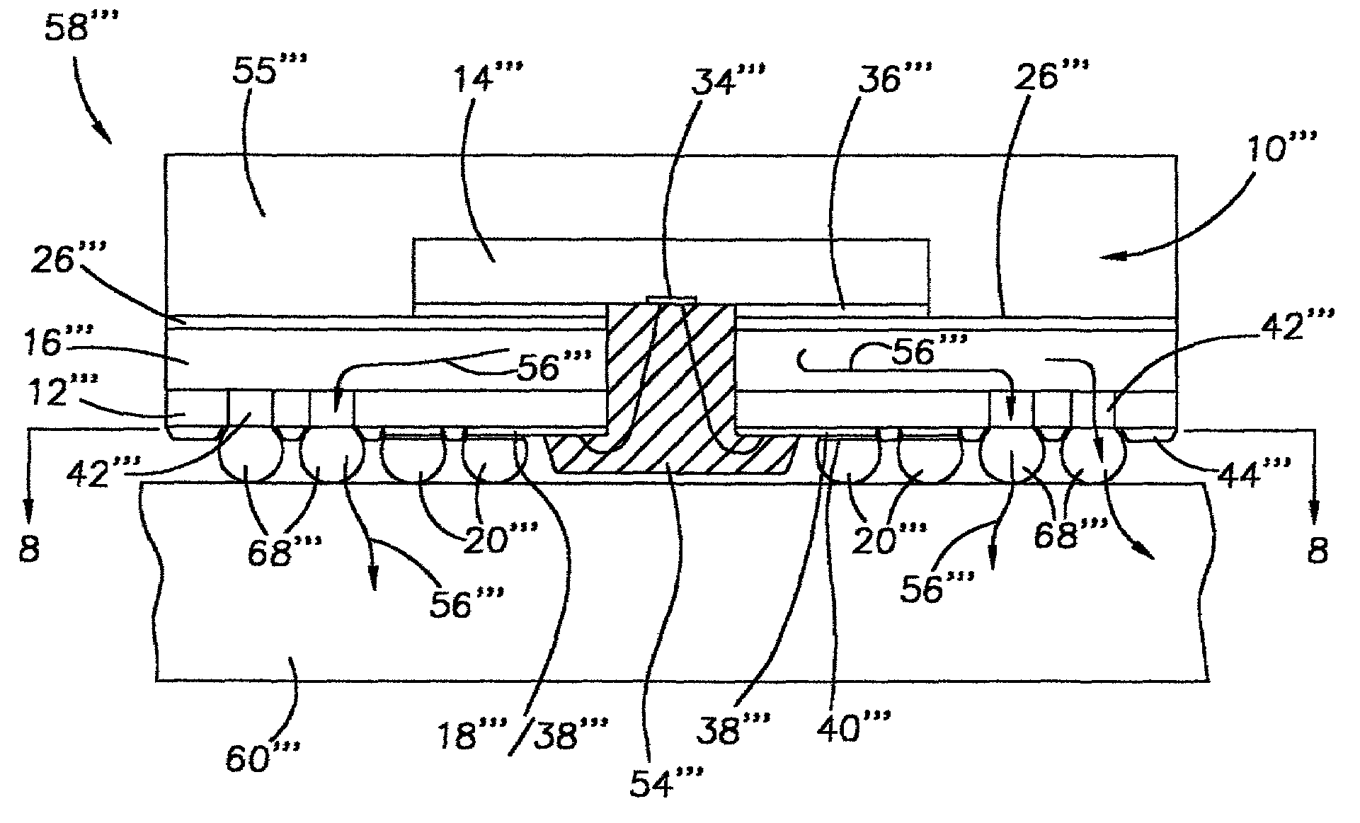
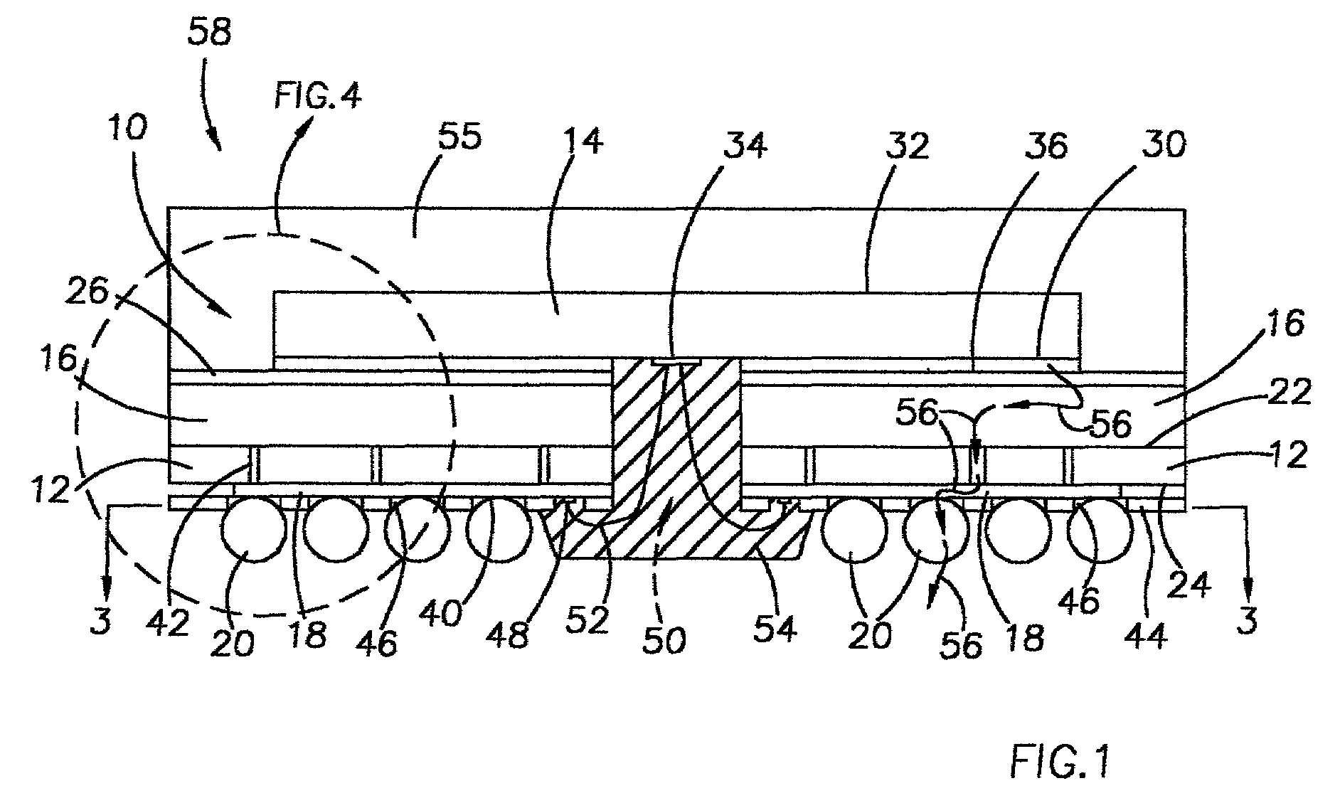
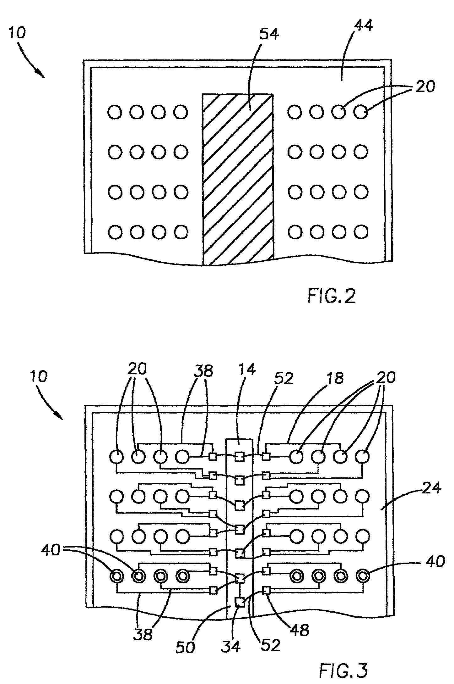
[0078]A sensitivity test study was conducted to determine the effects of substrate constructions and heat spreading attachments at natural and forced convection. The following substrate constructions were examined:[0079]a) A prior art semiconductor device 72 having a single metal layer construction (“single layer”), as depicted in FIG. 12. The device 72 comprised a support (core) substrate 12 made of bismaleimide triazine (BT) resin, a semiconductor die 14, a conductive (signal) plane layer 18 made of copper traces, and solder ball contacts 20.[0080]b) An embodiment of a semiconductor device according to the invention having a two metal layer construction (“2-layer”), as depicted in FIG. 1. The 2-layer device 10 had a thick copper plane layer 16, a support (core) substrate 12 made of BT resin, copper traces 18, and solder ball contacts 20.[0081]c) An embodiment of a semiconductor device according to the in...


PUM


Abstract

A semiconductor device for dissipating heat generated by a die during operation and having a low height profile, a semiconductor die package incorporating the device, and methods of fabricating the device and package are provided. In one embodiment, the semiconductor device comprises a thick thermally conductive plane (e.g., copper plane) mounted on a thin support substrate and interfaced with a die. Thermally conductive via interconnects extending through the substrate conduct heat generated by the die from the conductive plane to conductive balls mounted on traces on the opposing side of the substrate. In another embodiment, the semiconductor devices comprises a thick thermally conductive plane (e.g., copper foil) sandwiched between insulative layers, with signal planes (e.g., traces, bonding pads) disposed on the insulative layers, a die mounted on a first signal plane, and solder balls mounted on bonding pads of a second signal plane. A thermally conductive via interconnect extends through the substrate to provide a thermal path from the die and signal plane (traces) through the thick conductive plane and into the solder balls and external device (e.g., mother board). The present semiconductor device provides effective heat dissipation without the attachment of an external heat sink or spreader.

Description

FIELD OF THE INVENTION[0001]This invention relates in general to semiconductor devices and, more particularly, to a semiconductor device assembly having a integral heat sink for high power dissipation.BACKGROUND OF THE INVENTION[0002]An important characteristic of an electronic package is its ability to transfer heat out of the integrated circuit (IC) chip in order to ensure its proper operation and reliability. A considerable amount of heat is generated by the internal and surface circuits including transistors, resistors, capacitors, and other electronic components of an integrated circuit (IC) device. Fine ball grid arrays (FBGA) have superior electrical performance and has gained in popularity in memory packaging. As semiconductor devices become more dense, heat generation has greatly increased, requiring package construction that will transfer heat out of the IC chip in order to ensure its proper operation and reliability. However, the smaller package outline of an FBGA reduces...

Claims


Application Information

Patent Timeline
Patent Type & Authority Patents(United States)
IPC IPC(8): H01L23/34H01L23/10H01L23/36H01L23/31H01L23/367
CPCH01L23/3128H01L23/36H01L23/3677H01L24/49H01L24/45H01L2224/45144H01L2224/48091H01L2224/4824H01L2224/49112H01L2924/01005H01L2924/01006H01L2924/01013H01L2924/01014H01L2924/01027H01L2924/01028H01L2924/01029H01L2924/01039H01L2924/01046H01L2924/01047H01L2924/0105H01L2924/01073H01L2924/01074H01L2924/01075H01L2924/01078H01L2924/01079H01L2924/01082H01L2924/14H01L2924/15311H01L2924/19041H01L2924/00014H01L24/48H01L2224/32225H01L2224/48227H01L2224/73215H01L2224/73265H01L2924/01019H01L2924/01033H01L2924/01087H01L2924/014H01L2924/00012H01L24/73H01L2224/05554H01L2924/15747H01L2924/181H01L2924/351H01L2924/00
Inventor YEE, PAK HONGLEE, TECK KHENG
Owner MICRON TECH INC
Why Eureka
Try Eureka