Semiconductor device and method of manufacturing the same

a technology of semiconductors and semiconductors, applied in the direction of semiconductor devices, electrical devices, transistors, etc., can solve the problems of high production cost, high production cost, and high production cost, and achieve the effects of controlling the growth rate of the first substance, uniform growth rate, and uniform film thickness

Inactive Publication Date: 2006-11-28
LAPIS SEMICON CO LTD
View PDF3 Cites 2 Cited by
  • Summary
  • Abstract
  • Description
  • Claims
  • Application Information

AI Technical Summary

Benefits of technology

[0019]According to the semiconductor device, it is possible to control the growth rate of the first substance for epitaxial growth by forming either a third region that is made of the first substance and is formed on the surface of the second insulating film in a condition in which the surface is exposed for epitaxial growth, or a third region that is made of the first substance and is buried in the second insulating film in a condition such that the surface is exposed for epitaxial growth. The growth rate is also controlled by adjusting the exposed area of the first substance that is exposed on the substrate pattern for epitaxial growth. Further, if the area of exposed silicon is adjusted by the third region so that the density of exposed silicon can be uniform according to the layout for an identical chip, an identical wafer, or plurality of wafers for an identical process is conducted, it is possible to have a uniform growth rate on the identical chip, the identical wafer, or plurality of wafers on which the identical process is conducted and to have a uniform film thickness for the epitaxial layer.

Problems solved by technology

If the area of the active region is too small compared to the area of the trench in polishing the device-separation insulating film, there is a possibility that excessive of erosion may occur in the polish in the active region compared to the polish in the insulating film.
Also, in polishing the device-separation insulating film that is buried in a wide trench, there is a possibility dishing might occur in the thickness of the device-separation insulating film as the middle gets thinner than at the edges.
However, the problem of the growth rate in low-temperature epitaxial growth depending on the density of exposed silicon is described neither Japanese Patent Publications JP-A-2000-150806 and JP-A-11-003992, nor the nonpatent literature described above.

Method used


Image

  • Semiconductor device and method of manufacturing the same
  • Semiconductor device and method of manufacturing the same
  • Semiconductor device and method of manufacturing the same

Examples


first embodiment

[0040]In a first preferred embodiment of the present invention, an area of exposed silicon is adjusted by forming a pseudo electrode on a device-separation insulating film.

[0041]FIGS. 3 through 5 are views of cross-section diagrams illustrating a manufacturing method of an SOI semiconductor device in accordance with the first embodiment of the present invention. An example of the SOI semiconductor device is a full depletion layer type SOI semiconductor device that operates in a full depletion layer. In addition, the SOI semiconductor device can be a partial depletion layer type SOI semiconductor device. The present invention is especially effective for an SOI semiconductor device in which the SOI layer is extremely thinly formed (e.g., 50 nanometers or less), but it can be applied to any semiconductor device if it is manufactured by a manufacturing method including low-temperature epitaxial growth that is described below.

[0042]As shown in line (a) of FIG. 3, an SOI substrate, which ...

second embodiment

[0057]In a second preferred embodiment of the present invention, an area of exposed silicon is adjusted by forming a pseudo region on a device-separation insulating film.

[0058]FIGS. 6 though 8 are cross-section diagrams used to explain a method of manufacturing an SOI semiconductor device in accordance with the second embodiment of the present invention.

[0059]As shown in line (a) of FIG. 6, an SOI substrate that is identical or similar to the one that is used in the first embodiment of the present invention is prepared.

[0060]Next, as shown in line (b) of FIG. 6, a device-separation insulating film 4, which is made of silicon oxide, is formed by locally oxidizing silicon in a semiconductor layer 3 with a heretofore known Local Oxidation of Silicon (LOCOS) method. However, in the present embodiment, a pseudo region or regions 5b are also formed in addition to a device region 5a, which is separated by the device-separation insulating film 4. The device region 5a is a region in which an...

third embodiment

[0072]In a preferred third embodiment of the present invention, an area of exposed silicon is adjusted by forming both a pseudo electrode and a pseudo region on a device-separation insulating film.

[0073]FIGS. 9 through 11 are cross-section diagrams used to explain a method of manufacturing an SOI semiconductor device in accordance with the third embodiment of the present invention.

[0074]As shown in line (a) of FIG. 9, an SOI substrate that is identical or similar to that of the first embodiment of the present invention is prepared.

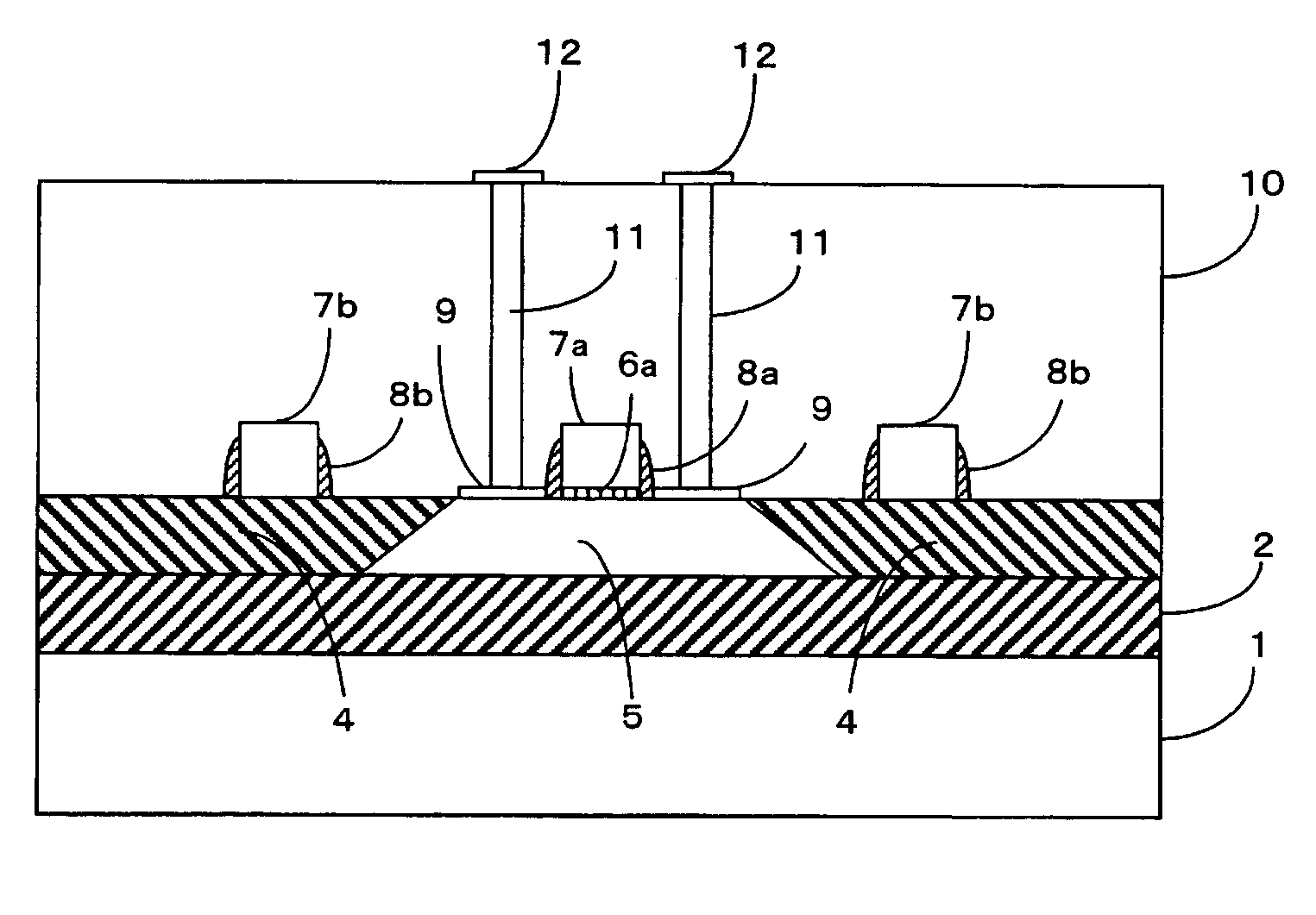
[0075]Next, as shown in line (b) of FIG. 9, a device-separation insulating film 4 is formed in a semiconductor layer 3 and a device region 5a and a pseudo region 5b are formed preferably in the same way as those of the second embodiment of the present invention.

[0076]Next, as shown in line (c) of FIG. 9, insulating films 6a and 6b that are made of silicon oxide are respectively formed on the surface of the device region 5a and the pseudo region 5b. Further...


PUM


Abstract

A method of manufacturing a semiconductor device includes a step of forming a device region 5 that is separated by a device-separation insulating film 4 formed in a part of an SOI layer, a step of forming a gate insulating film 6a on a device region 5 so that the device region 5 can be exposed on both sides of the gate insulating film 6a, a step of forming a gate electrode 7a with polysilicon on the gate insulating film 6a, a step of adjusting the area of exposed silicon so that the area of exposed silicon can be a prescribed area by forming at least either a pseudo region 5b or a pseudo electrode 7b to control the growth rate in growing an epitaxial layer 9, and a step of conducting low-temperature epitaxial growth of silicon.

Description

BACKGROUND OF THE INVENTION[0001]1. Field of the Invention[0002]The present invention relates to a semiconductor device and a method of manufacturing the same. More specifically, the present invention relates to a semiconductor device that includes a device formed in a semiconductor layer on an insulating film, and a method of manufacturing the same.[0003]2. Background Information[0004]Related examples of a semiconductor device that include an MOS transistor formed with a semiconductor process are described in Japanese Patent Publications JP-A-2000-150806 and JP-A-11-003992, which are hereby incorporated by reference.[0005]Japanese Patent Publication JP-A-2000-150806 discloses a semiconductor device, which includes device-separation insulating films, an active region, a pseudo region, a gate electrode, a pseudo conductive film, and an interlayer insulating film. The device-separation insulating films are buried in trenches formed on a surface of a semiconductor substrate of a bulk. ...

Claims


Application Information

Patent Timeline
Patent Type & Authority Patents(United States)
IPC IPC(8): H01L21/84H01L29/786H01L21/28H01L21/336H01L27/108H01L27/12H01L29/78
CPCH01L29/7834H01L21/28123H01L21/84H01L27/1203H01L29/66628
Inventor OKAMURA, TOMOHIRO
Owner LAPIS SEMICON CO LTD
Why Eureka
Try Eureka