Apparatus for imprinting lithography and fabrication thereof

a technology of imprinting lithography and apparatus, which is applied in the direction of electrical apparatus, semiconductor/solid-state device manufacturing, and semiconductor devices, etc., can solve the problems of crystal degradation to the mold material, e-beam lithography is slow and therefore of limited use in high throughput or production situations, and the resolution of e-beam lithography is limited in the nano-scale rang

Inactive Publication Date: 2006-11-28
HEWLETT PACKARD DEV CO LP
View PDF7 Cites 27 Cited by
  • Summary
  • Abstract
  • Description
  • Claims
  • Application Information

AI Technical Summary

Problems solved by technology

However, e-beam lithography is slow and therefore of limited use in high throughput or production situations.
Moreover, e-beam lithography has limited resolution in the nano-scale range.
Further, the RIE process causes crystal degradation to the mold material.
While holding much promise, the practical use of such fabricated molds has been somewhat limited.
In particular, the sur

Method used


Image

  • Apparatus for imprinting lithography and fabrication thereof
  • Apparatus for imprinting lithography and fabrication thereof
  • Apparatus for imprinting lithography and fabrication thereof

Examples


Embodiment Construction

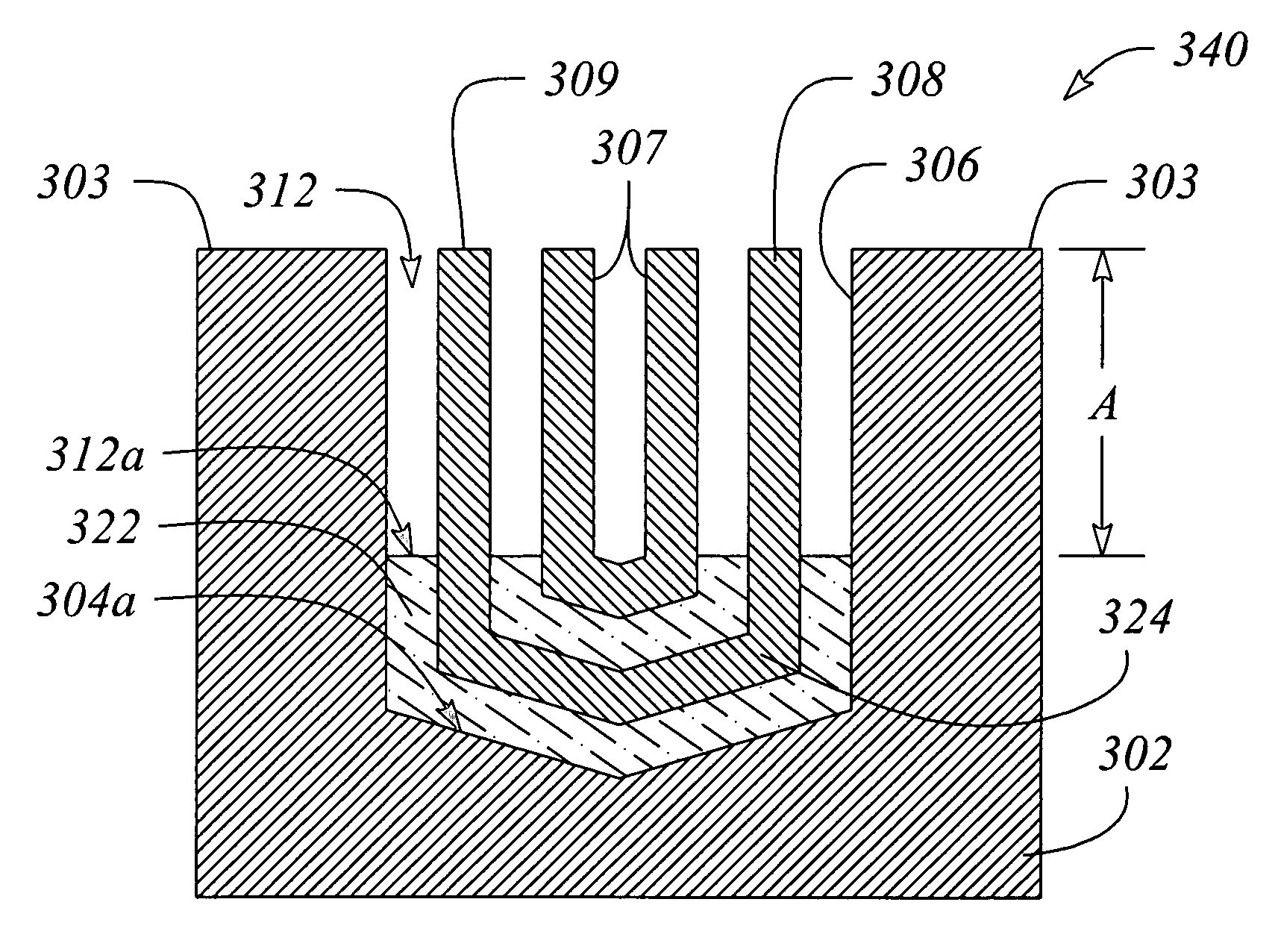
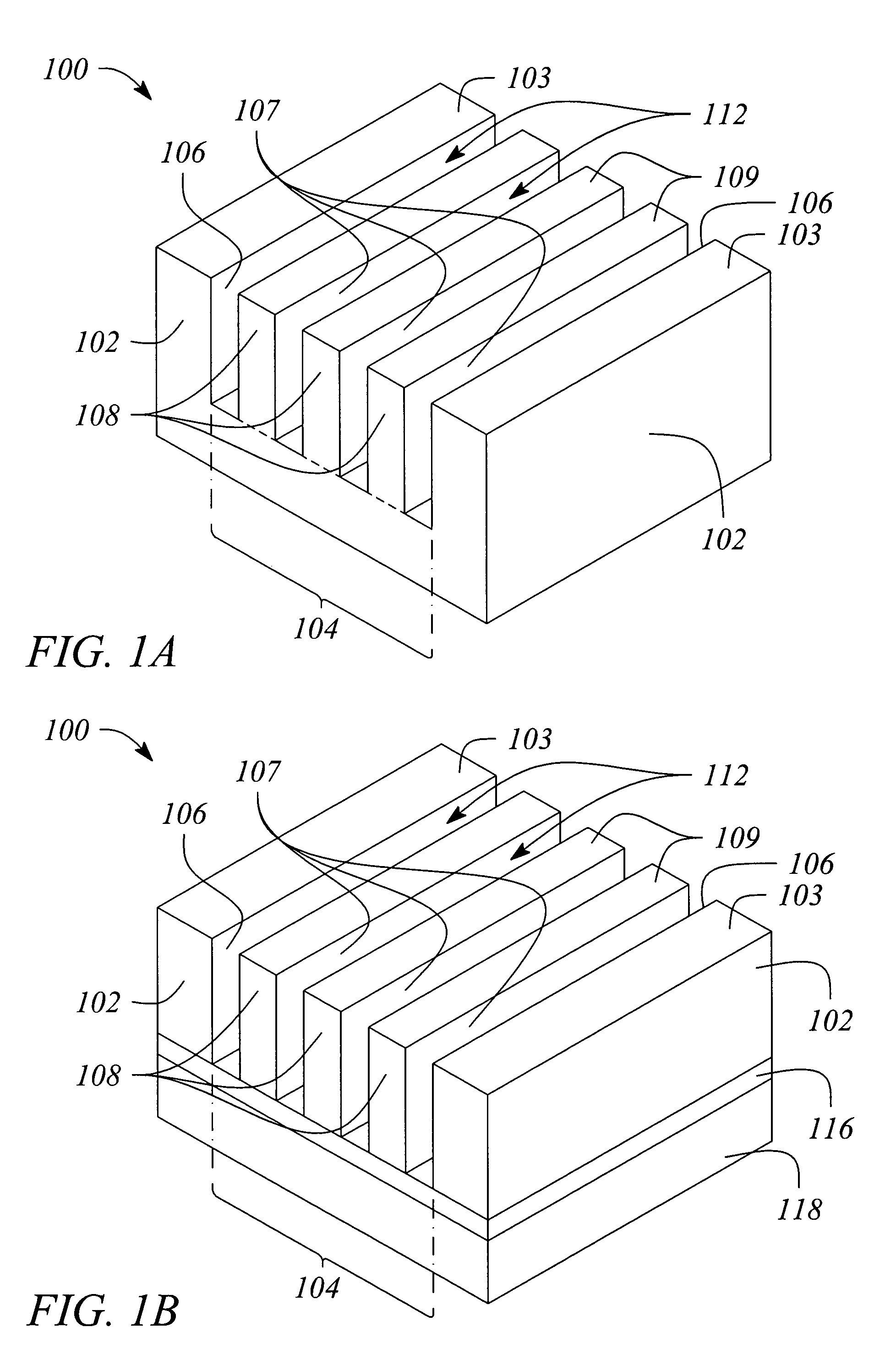
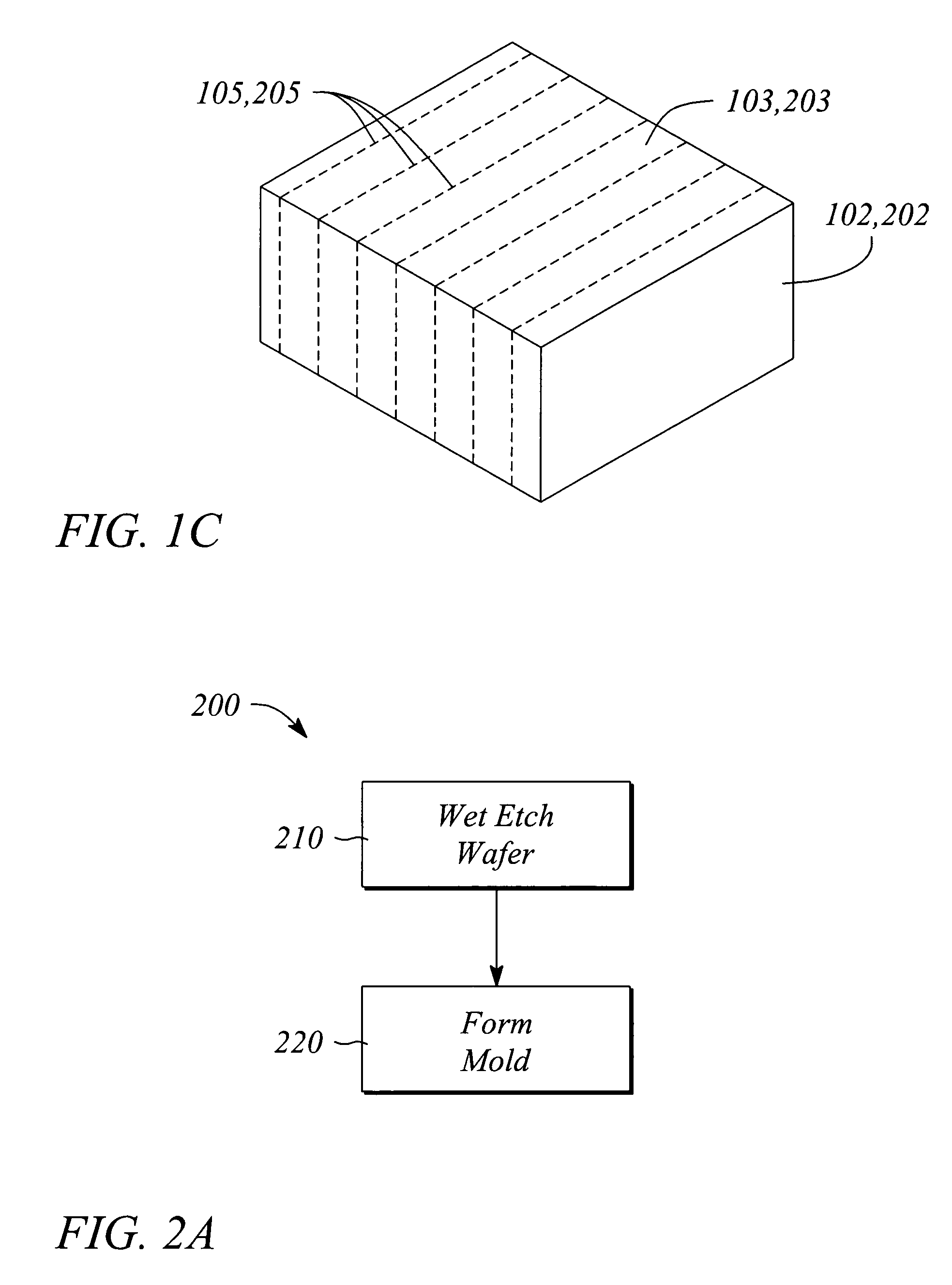
[0026]FIG. 1A illustrates a perspective view of an embodiment of an imprinting apparatus 100 in accordance with an embodiment of the present invention. FIG. 1B illustrates a perspective view of another embodiment of an imprinting apparatus 100 in accordance with an embodiment of the present invention. The apparatus 100 is a nano-imprinting mold 100 having formed therein one or both of a nano-scale mold pattern and a micro-scale mold pattern that, when imprinted on a substrate surface, facilitates forming structures, such as nanowires or other circuit elements, on the substrate surface. The techniques for nano-imprinting with molds are known for example, from U.S. Pat. Nos. 5,772,905; 6,309,580; 6,294,450 and 6,407,443, all of which are incorporated herein by reference in their entirety. Such nano-imprinting techniques are applicable to micro-scale imprinting as well. Therefore while the following description uses the term or prefix ‘nano’ throughout, in accordance with the various e...


PUM


Abstract

An imprinting apparatus and method of fabrication provide a mold having a pattern for imprinting. The apparatus includes a semiconductor substrate polished in a [110] direction. The semiconductor substrate has a (110) horizontal planar surface and vertical sidewalls of a wet chemical etched trench. The sidewalls are aligned with and therefore are (111) vertical lattice planes of the semiconductor substrate. The semiconductor substrate includes a plurality of vertical structures between the sidewalls, wherein the vertical structures may be nano-scale spaced apart. The method includes wet etching a trench with spaced apart (111) vertical sidewalls in an exposed portion of the (110) horizontal surface of the semiconductor substrate along (111) vertical lattice planes. A chemical etching solution is used that etches the (111) vertical lattice planes slower than the (110) horizontal lattice plane. The method further includes forming the imprinting mold.

Description

BACKGROUND[0001]1. Technical Field[0002]The invention relates to the fabrication of nano-scale and micro-scale structures. In particular, the invention relates to molds used in imprinting lithography.[0003]2. Description of Related Art[0004]A consistent trend in semiconductor technology since its inception is toward smaller and smaller device dimensions and higher and higher device densities. As a result, an area of semiconductor technology that recently has seen explosive growth and generated considerable interest is nanotechnology. Nanotechnology is concerned with the fabrication and application of so-called nano-scale structures, structures having dimensions that are often 50 to 100 times smaller than conventional semiconductor structures. Nano-imprinting lithography is a technique used to fabricate nano-scale structures.[0005]Nano-imprinting lithography uses a mold to imprint nano-scale structures on a substrate. A mold typically contains a plurality of protruding and / or recesse...

Claims


Application Information

Patent Timeline
IPC IPC(8): H01L29/04H01L31/036
CPCH01L21/0337H01L21/76838
Inventor ISLAM, M. SAIFJUNG, GUN YOUNGCHEN, YONGWILLIAMS, R. STANLEY
Owner HEWLETT PACKARD DEV CO LP
Why Eureka
Try Eureka