Display device and manufacturing method of the same

a display device and flat panel technology, applied in the direction of identification means, semiconductor/solid-state device details, instruments, etc., can solve the problems of degeneration of display quality and difficult accurate recognition of the position of gold bumps, and achieve accurate alignment of bumps formed, prevent the deterioration of display quality, and facilitate the recognition of the profile of gold bumps of drive circuit chips.

Active Publication Date: 2006-11-28
JAPAN DISPLAY INC +1
View PDF2 Cites 18 Cited by
  • Summary
  • Abstract
  • Description
  • Claims
  • Application Information

AI Technical Summary

Benefits of technology

[0007]In this type of drive circuit chip, the alignment mark is formed on the conductive layer ALL and there exists the positional displacement or the misalignment of approximately 5 μm with respect to the positional relationship between the alignment mark and the bump. Then, a profile of the conductive layer ALL which is connected to the gold bump A-BMP is set larger than the shape of the gold bump A-BMP and projects from the gold bump A-BMP. Accordingly, the position measurement of the gold bump is influenced by the profile of the conductive layer ALL thus making the accurate recognition of the position of the gold bump difficult. Accordingly, even when the mounting of the drive circuit chip is performed by aligning the driver circuit chip and the substrate while recognizing the alignment mark, there arises the irregularities of the misalignment of the above-mentioned approximately 5 μm between the gold bumps of the drive circuit chip and the alignment mark. As a result, the mounting accuracy of the drive circuit chip on the substrate is lowered thus giving rise to the degeneration of the display quality.
[0008]The present invention has an advantage that the present invention can provide a flat-panel-type display device and a manufacturing method thereof which can realize the high-quality display by enhancing the mounting accuracy of the drive circuit chip.
[0009]The present invention uses a bump (for example, a gold bump) of a drive circuit chip for alignment. Here, to enhance the recognition property of the alignment bump, a plane shape of a conductive layer which is formed between a semiconductor substrate (Si substrate) of the drive circuit chip and the alignment bump is configured to be included within a profile of a plane shape of the alignment bump. That is, by preventing the conductive layer from being observed in the periphery of the alignment bump, it is possible to prevent the conductive layer from influencing a photographed pattern of the bump taken by a camera or the like.
[0035]According to the present invention, the recognition of the profile of the bump of the drive circuit chip is facilitated and hence, at the time of mounting the drive circuit chip on the substrate, it is possible to accurately align the bumps formed on the drive circuit chip and wiring electrodes of the substrate on which the drive circuit chip is mounted (for example, the substrate (for example, TFT substrate) of the display panel, printed circuit board, flexible printed circuit board or the like) whereby it is possible to prevent the deterioration of the display quality attributed to the defective mounting of the drive circuit chip.

Problems solved by technology

Accordingly, the position measurement of the gold bump is influenced by the profile of the conductive layer ALL thus making the accurate recognition of the position of the gold bump difficult.
As a result, the mounting accuracy of the drive circuit chip on the substrate is lowered thus giving rise to the degeneration of the display quality.

Method used


Image

  • Display device and manufacturing method of the same
  • Display device and manufacturing method of the same
  • Display device and manufacturing method of the same

Examples


embodiment 1

[Embodiment 1]

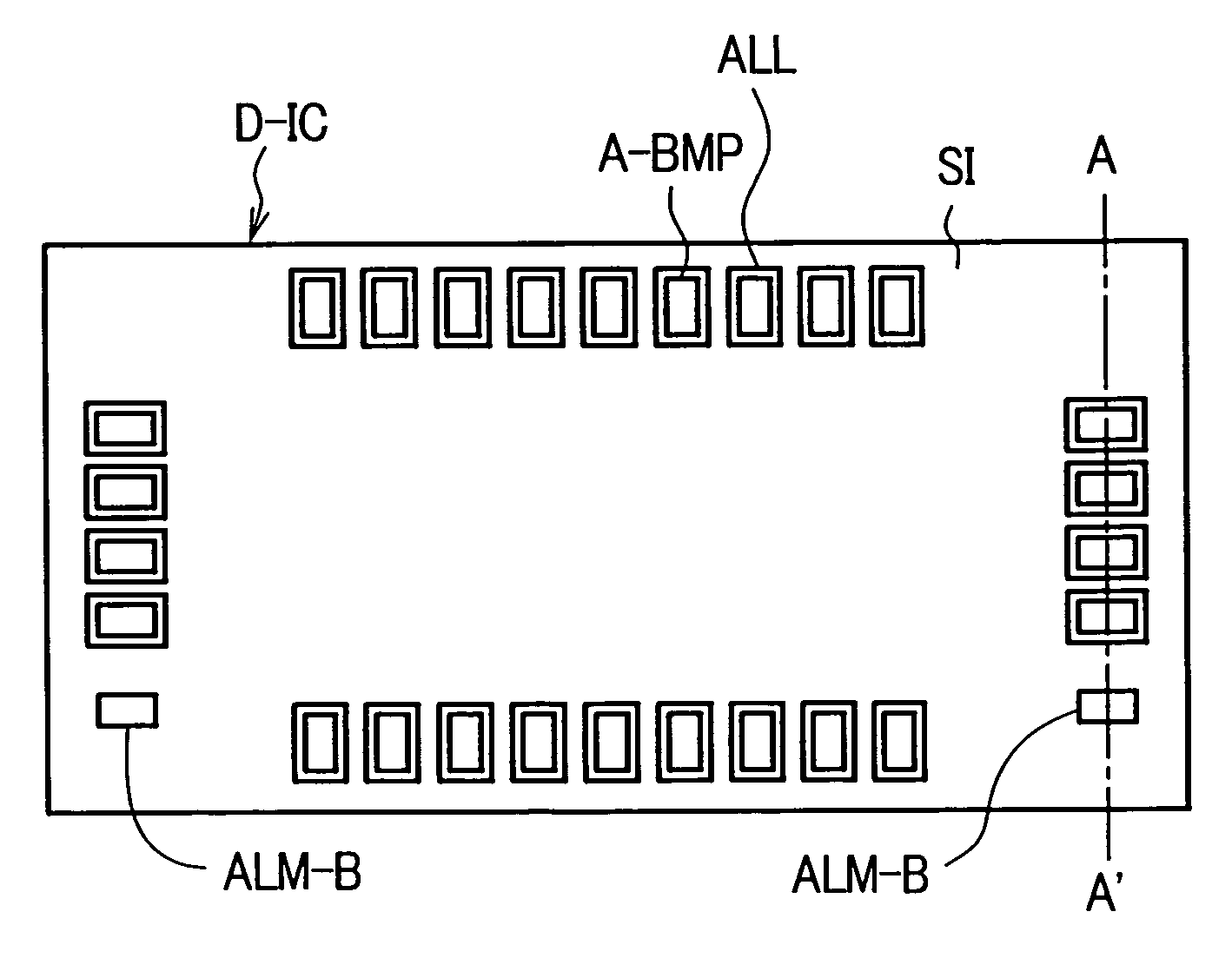
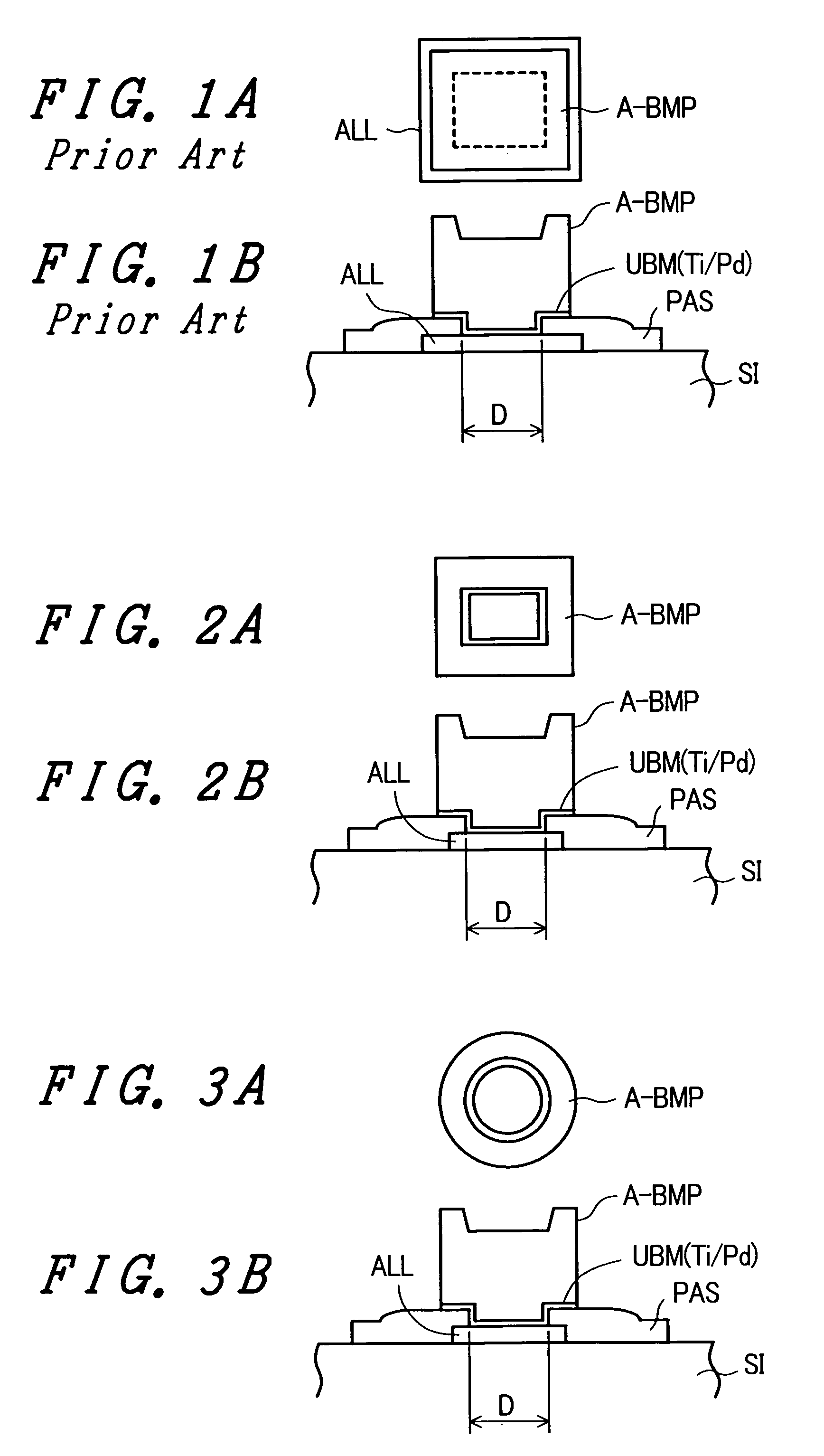
[0051]FIG. 2A and FIG. 2B are views for explaining the embodiment 1 of the present invention, wherein FIG. 2A is a plan view and FIG. 2B is a cross-sectional view. Reference symbols equal to the reference symbols used in FIG. 1A and FIG. 1B correspond to same functional parts. In the present invention, a gold bump A-BMP per se is used as an alignment mark. In this embodiment, the bump which is used as the alignment mark (alignment bump) is formed in a small plane shape (a rectangular shape) such that, as viewed on a plane parallel to a surface of an Si substrate SI, a plane shape of the gold bump A-BMP assumes a rectangular shape and a profile shape of a conductive layer ALL is included within a profile of the gold bump A-BMP. Here, in FIG. 2B, although a background metal layer UBM has the same plane shape (rectangular shape) as the profile of the gold bump A-BMP, this background metal layer UBM may have a small plane shape such that the background metal layer UBM also...

embodiment 2

[Embodiment 2]

[0057]FIG. 3A and FIG. 3B are views for explaining the embodiment 2 of the present invention, wherein FIG. 3A is a plan view and FIG. 3B is a cross-sectional view. Reference symbols equal to the reference symbols used in FIG. 2A and FIG. 2B correspond to same functional parts. In this embodiment, as viewed on a plane parallel to a surface of an Si substrate SI, a planer shape of the gold bump A-BMP assumes a circular shape. Further, a background metal layer UBM and conductive layers ALL formed below the gold bump A-BMP are substantially equal to the background metal layer UBM and the conductive layers ALL of the embodiment 1 except for a point that the background metal layer UBM and the conductive layers ALL have a circular shape in plan.

embodiment 3

[Embodiment 3]

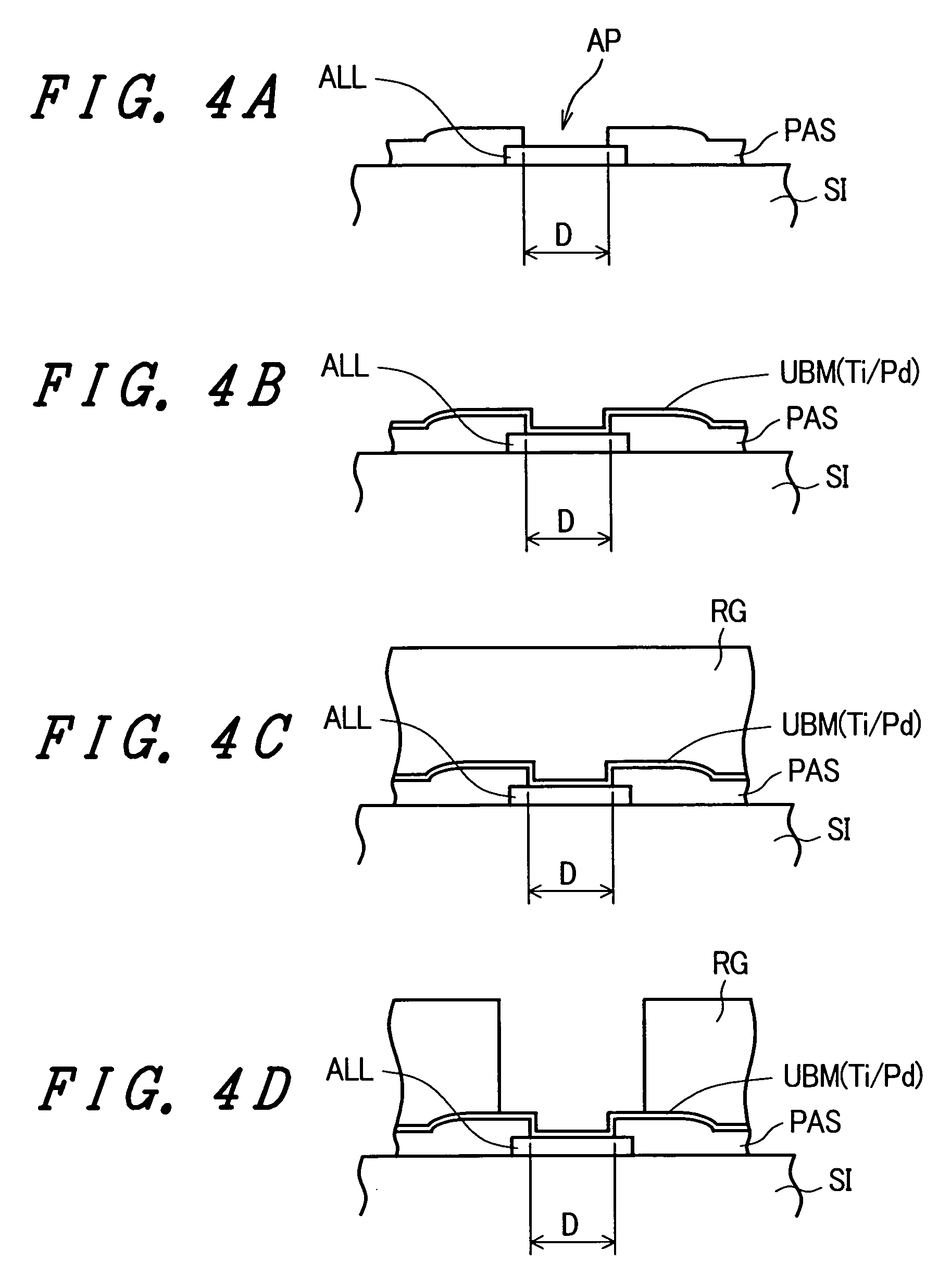
[0058]FIG. 14A and FIG. 14B are views for explaining the embodiment 3 of the present invention, wherein FIG. 14A is a plan view and FIG. 14B is a cross-sectional view. Reference symbols equal to the reference symbols used in FIG. 2A and FIG. 2B correspond to same functional parts. This embodiment adopts the structure in which only a background layer UBM is formed below an alignment bump and a conducive layer ALL is not formed. Here, since conductive layers ALL are formed below input bumps and output bumps as usual, in this structure, the number of conductive layers (the background metal layer UBM) formed between the semiconductor substrate (Si substrate SI) and the alignment bump is set smaller than the number of conductive layers (the conductive layers ALL and the background metal layer UBM) formed between the semiconductor substrate (Si substrate SI) and the output bumps. Although a height of the alignment bump becomes lower than a height of the output bumps by appro...


PUM

PropertyMeasurementUnit
heightaaaaaaaaaa
sizeaaaaaaaaaa
sizeaaaaaaaaaa

Abstract

The present invention enhances the mounting accuracy of a drive circuit chip on a substrate thus realizing a display of high quality. Bumps (for example, gold bumps) on the drive circuit chip are used for alignment. Here, to enhance the recognition property of the alignment bumps, a plane shape of a conductive layer which is formed between a semiconductor substrate (Si substrate) of the drive circuit chip and the alignment bump is set to be included within a profile of a plane shape of the alignment bump. That is, by preventing the conductive layer from being observed in a periphery of the alignment bump, it is possible to prevent a photographed pattern of the bump taken by a camera or the like from be influenced by the conductive layer.

Description

[0001]The present application claims priority from Japanese application JP2004-119263 filed on Apr. 14, 2004, the content of which is hereby incorporated by reference into this application.BACKGROUND OF THE INVENTION[0002]The present invention relates to a flat-panel-type display device using a display panel and a manufacturing method thereof, and is preferably applicable to a display device which mounts a drive circuit chip thereon with high accuracy.[0003]Various types of flat-panel type display devices such as a display device which is capable of performing a high-definition color display for a notebook type computer or a display monitor or a liquid crystal display device which uses a liquid crystal panel, an organic electroluminescence display device (an organic EL display device) which uses electroluminescence (particularly organic electroluminescence) elements or a field emission type display device (FED) which uses field emission elements as a display panel for a mobile phone...

Claims


Application Information

Patent Timeline
Patent Type & Authority Patents(United States)
IPC IPC(8): H01L23/48G02F1/1345H01L21/60G02F1/13G02F1/133G09F9/00G09G3/36H01L21/44H01L23/485H01L23/544
CPCH01L24/05H01L24/11H01L24/29H01L24/03H01L24/12H01L24/17H01L24/83G02F1/13452H01L23/544H01L2224/81136H01L2924/07811H01L2224/13019H01L2224/0554H01L2224/05001H01L2224/05555H01L2224/05553H01L2924/00013H01L2224/293H01L2224/2929H01L2224/81903H01L2224/83851H01L2224/13016H01L2223/5442H01L2223/54473H01L2223/5448H01L2224/0401H01L2224/1147H01L2224/13099H01L2224/13144H01L2224/838H01L2924/01004H01L2924/01005H01L2924/01006H01L2924/01013H01L2924/01014H01L2924/01018H01L2924/01022H01L2924/01033H01L2924/01046H01L2924/01078H01L2924/01079H01L2924/01082H01L2924/0781H01L2924/12044H01L2924/00014H01L2224/29099H01L2224/29199H01L2224/29299H01L2924/00H01L2224/8113H01L2224/81132H01L2924/181
Inventor ABE, HIDEAKISATO, MAKOTOGOTO, MITSURU
Owner JAPAN DISPLAY INC
Why Eureka
Try Eureka