Method for manufacturing metal structure having different heights

a manufacturing method and metal structure technology, applied in semiconductor devices, semiconductor/solid-state device details, electrical devices, etc., can solve the problems of contamination of substrate b>1/b>, process becomes very difficult and troublesome, and the whole process becomes very complicated, so as to achieve the effect of simplifying the manufacturing process and reducing the complexity of the mold forming process

Active Publication Date: 2006-12-12
SAMSUNG ELECTRONICS CO LTD
View PDF5 Cites 37 Cited by
  • Summary
  • Abstract
  • Description
  • Claims
  • Application Information

AI Technical Summary

Benefits of technology

[0016]An aspect of the present invention is to solve at least the above problems and / or disadvantages and to provide at least the advantages described below. Accordingly, an aspect of the present invention is to provide a method for manufacturing a metal structure having different heights, wherein the method is capable of achieving simplification of the whole process by minimizing the difficult and complicated process of forming the plating mold and performing the plating process.
[0021]According to embodiments of the present invention having the above construction, the plating mold forming process and the plating process which are complicated and difficult may be reduced, and therefore, the method for manufacturing a metal structure having different heights can be simplified.

Problems solved by technology

However, since the conventional method for manufacturing a metal structure having different heights requires a complicated photolithography process and a plating process that must be performed twice, respectively, in the formation of the first plating mold 3 and the second plating mold 5, the whole process becomes very complicated.
Thus, the process becomes very difficult and troublesome.
Additionally, the substrate 1 can be contaminated due to the frequent photolithography processes, and the plating for the second metal structure 6 may become unstable.
Therefore, the conventional process becomes even more complicated.

Method used


Image

  • Method for manufacturing metal structure having different heights
  • Method for manufacturing metal structure having different heights
  • Method for manufacturing metal structure having different heights

Examples


Embodiment Construction

[0025]Illustrative, non-limiting embodiments of the present invention will be described in greater detail with reference to the accompanying drawings.

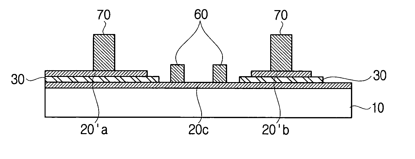
[0026]Referring to FIG. 2A through FIG. 2H, the characteristics of the method for manufacturing a metal structure having different heights according to an embodiment of the present invention is that a plurality of layers are formed in forming a plating base layer on a semiconductor substrate 10, for example, as shown in FIG. 2A, two seed layers (a first seed layer 20 and second seed layer 20′) are formed if the height difference of the metal structure to be formed is one step. The first seed layer 20 and the second seed layer 20′ are electrically separated by an insulating layer 30 that is interposed between the seed layers. Although the drawings show the case of employing two seed layers 20 and 20′, the number of the seed layers can be reduced or increased depending on the height difference of the metal structure to be formed.

[0027]An...


PUM

PropertyMeasurementUnit
heightsaaaaaaaaaa
insulatingaaaaaaaaaa
thicknessesaaaaaaaaaa

Abstract

Disclosed is a method for forming a plurality of metal structures having different heights on a semiconductor substrate. The disclosed method for manufacturing a metal structure having different heights includes: forming a plurality of seed layers, to have heights corresponding to the metal structure to be formed, on a semiconductor substrate so that those layers can be electrically separated, performing a plating process using a plating mold, and applying different currents to the respective seed layers so that the plating thickness can be adjusted for each of the seed layers. Accordingly, a plurality of metal structures having different heights can be obtained by a plating mold forming process and a plating process that are performed just once, respectively.

Description

CROSS-REFERENCE TO RELATED APPLICATIONS[0001]This application claims the benefit of Korean Application No. 2003-92620, filed Dec. 17, 2003, in the Korean Intellectual Property Office, the disclosure of which is incorporated herein by reference.BACKGROUND OF THE INVENTION[0002]1. Field of the Invention[0003]The present invention relates to a method for manufacturing a metal structure having different heights formed on a semiconductor substrate. For example, a portion of the metal structure is used for a semiconductor element, and another portion of the metal structure, having a different height, is used for packaging of the semiconductor element.[0004]2. Description of the Related Art[0005]Generally, a certain fine metal structure used for a semiconductor element needs to be packaged for protection. To accomplish this, a second fine metal structure having a height higher than the fine metal structure is usually formed on both sides of the fine metal structure for packaging the elemen...

Claims


Application Information

Patent Timeline
Patent Type & Authority Patents(United States)
IPC IPC(8): H01L21/44H01L21/288C25D7/12H01L21/3205H01L21/768H01L23/52
CPCH01L21/2885H01L21/76885H01L24/11H01L24/12H01L2224/0401H01L2224/0603H01L2224/13099H01L2224/1403H01L2924/01027H01L2924/01033H01L2924/01078H01L2924/01005H01L2924/01006H01L2924/181H01L2924/00C25D7/123C25D5/16
Inventor SHIM, DONG-SIKJUN, CHAN-BONGCHOI, HYUNGSONG, HOON
Owner SAMSUNG ELECTRONICS CO LTD
Why Eureka
Try Eureka