Semiconductor integrated circuit device

a technology of integrated circuits and semiconductors, applied in the direction of solid-state devices, pulse techniques, basic electric elements, etc., can solve the problems of interfering with the reduction of chip size, and influence of temperature, so as to reduce the size of the semiconductor integrated circuit chip

Inactive Publication Date: 2006-12-12
RENESAS TECH CORP
View PDF24 Cites 10 Cited by
  • Summary
  • Abstract
  • Description
  • Claims
  • Application Information

AI Technical Summary

Benefits of technology

[0016]This invention has been made to solve the foregoing drawbacks. It is therefor an object of the present invention to obtain a semiconductor integrated circuit device capable of easily and reliably connecting bonding wires between PADs and LEADs.
[0017]It is another object of the present invention to obtain a semiconductor integrated circuit device that ensures the supply of stable power.
[0020]Thus, wiring for long bonding wires extending across the one semiconductor integrated circuit chip can be eliminated, and electrical connections of the bonding wires between the PADs and LEADs are made easily and reliably.
[0022]Thus, since wiring is made between one LEAD and two PADs, the number of LEADs to be used can be reduced.
[0028]Thus, a temperature distribution lying within the semiconductor integrated circuit chip is recognized and estimated, thereby reducing the size of the semiconductor integrated circuit chip.

Problems solved by technology

There arises a drawback in that-since the conventional semiconductor integrated circuit device is constructed as described above, a further reduction in chip size where a plurality of chips are mounted, will cause a difficulty in connecting bonding wires between PADs of a chip and LEADs at positions where the PADs of the chip and the LEADs do not adjoin, when the number of the bonding wires is identical or increases, thereby interfering with the reduction in chip size.
There also arises a drawback in that a further reduction in chip size where a plurality of chips are mounted, will cause a difficulty in supplying stable power at positions where PADs of a chip and LEADs do not adjoin, when the number of bonding wires is identical or increases, thereby interfering with the reduction in chip size.
Further, there arises a drawback in that since a plurality of chips are disposed adjacent to one another, the influence of temperatures on the respective chips by heat generation of the chips cannot be avoided, and when a chip size is further reduced, the condition of a chip-in temperature distribution must be confirmed from the need for taking into consideration the above influence of temperatures on the respective chips.

Method used


Image

  • Semiconductor integrated circuit device
  • Semiconductor integrated circuit device
  • Semiconductor integrated circuit device

Examples


first embodiment

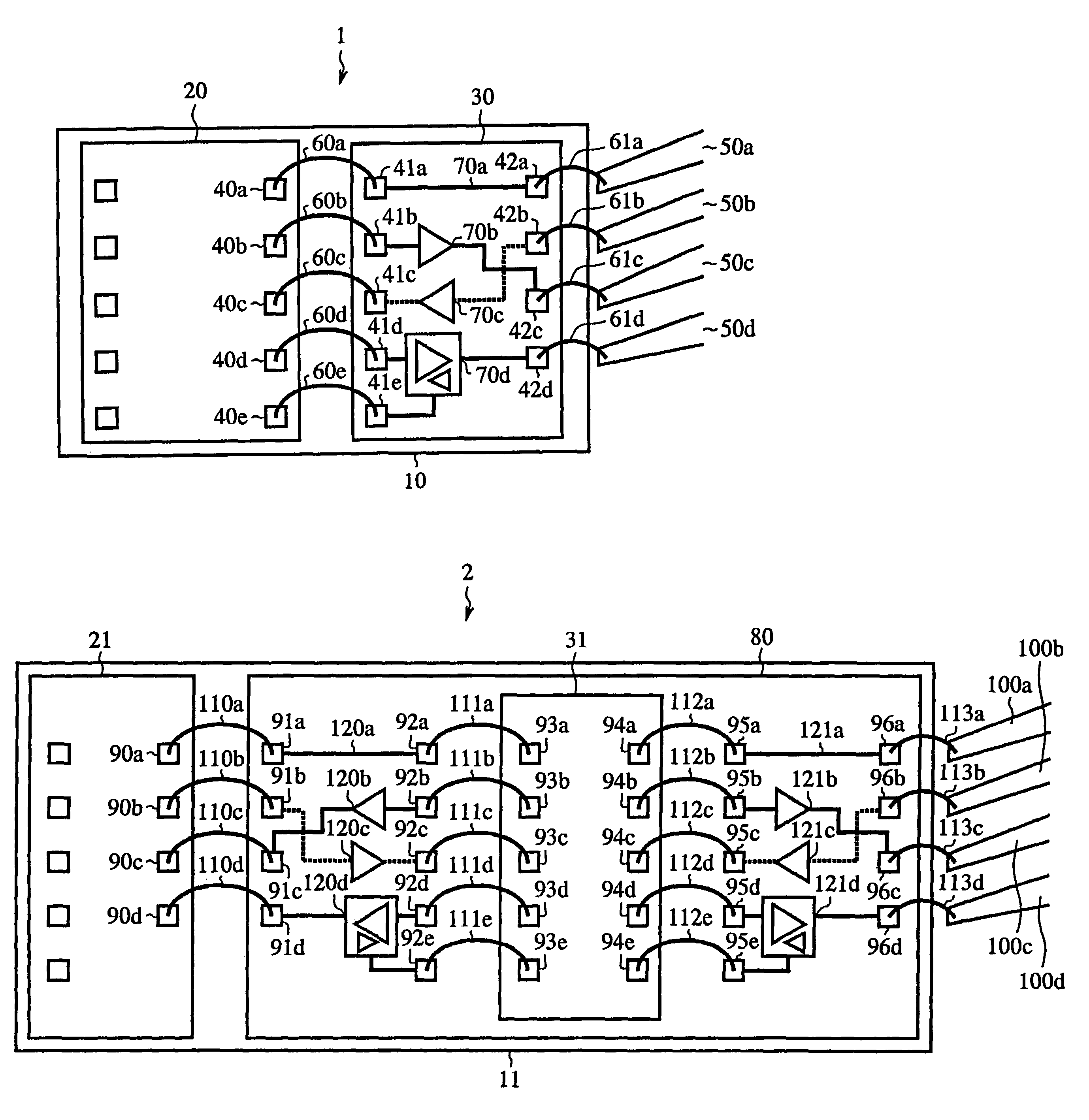
[0049]FIG. 1 is a plan view showing a semiconductor integrated circuit device according to a first embodiment of the present invention. In FIG. 1, reference numeral 1 indicates a semiconductor integrated circuit device. Reference numeral 10 indicates a bonding pad (bonding PAD), reference numeral 20 indicates a semiconductor integrated circuit chip A (Chip. A) disposed on the bonding PAD 10, and reference numeral 30 indicates a semiconductor integrated circuit chip B (Chip B) including interface functions (I / F functions), which is disposed on the bonding PAD 10, respectively. Reference numerals 40a–40e indicate pads (PADs) of the Chip A20, and reference numerals 41a–41e and 42a–42d indicate pads (PADs) of the Chip B30, respectively. Reference numerals 50a–50d indicate leads (LEADs) disposed around arrays of the Chip A20 and Chip B30 disposed on the bonding PAD 10. Reference numerals 60a–60e and 61a–61d respectively indicate bonding wires. Reference numeral 70a indicates a wiring ele...

second embodiment

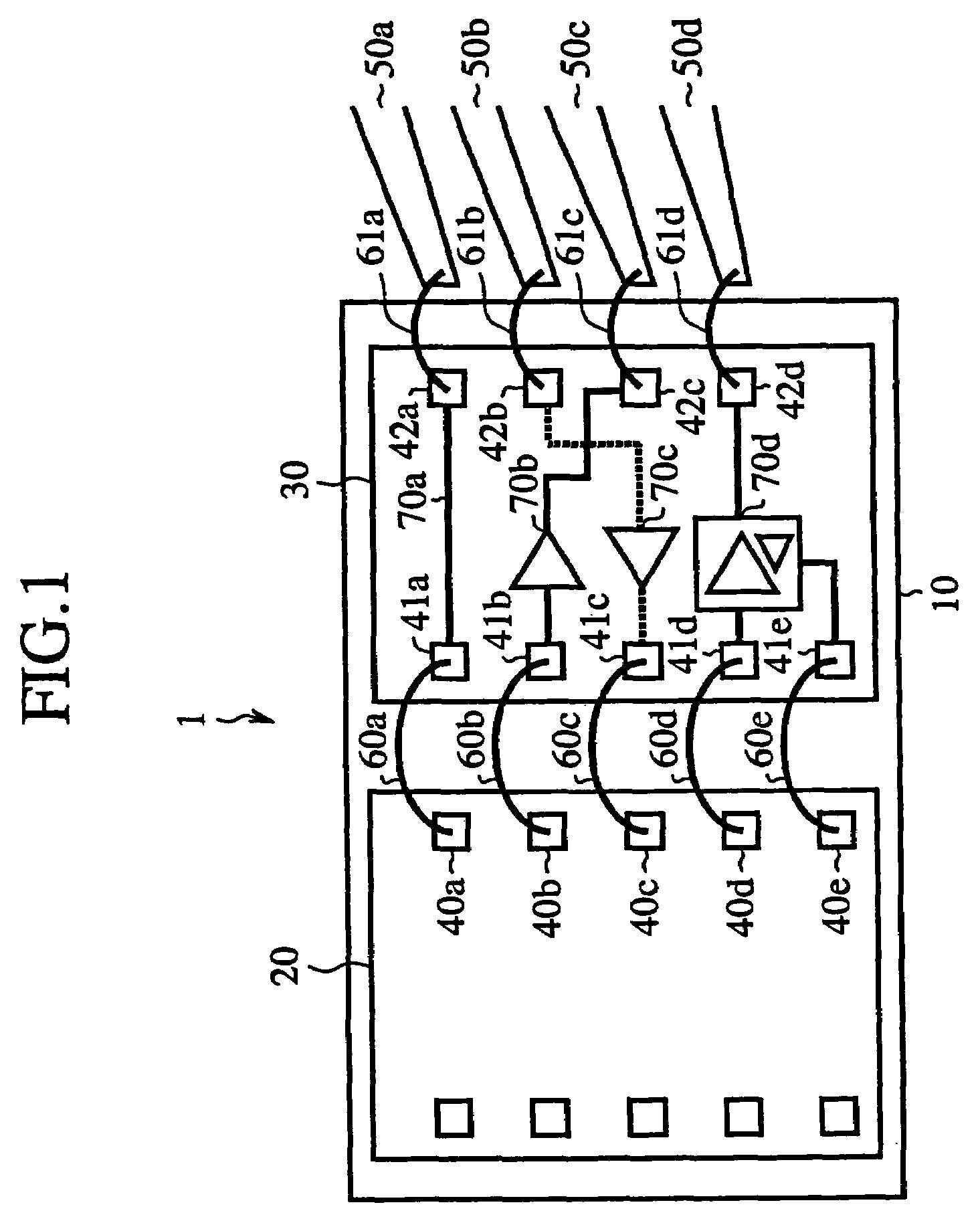
[0064]FIG. 2 is a plan view showing a semiconductor integrated circuit device according to a second embodiment of the present invention. In FIG. 2, reference numeral 2 indicates a semiconductor integrated circuit device. Reference numeral 11 indicates a bonding pad (bonding PAD), reference numeral 21 indicates a semiconductor integrated circuit chip A (Chip A) disposed on the bonding PAD 11, reference numeral 80 indicates a semiconductor integrated circuit chip (I / F Chip) including interface functions (I / F functions), which is disposed on the bonding PAD 11, and reference numeral 31 indicates a semiconductor integrated circuit chip (Chip B) disposed between portions where the I / F functions of the I / F chip80 are provided, respectively. Reference numerals 90a–90d indicate pads (PADs) of the Chip A21, reference numerals 91a–91d, 92a–92e, 95a–95e and 96a–96dindicate pads (PADs) of the I / F Chip80, and reference numerals 93a–93e and 94a–94e indicate pads (PADs) of the Chip B31, respective...

third embodiment

[0083]FIG. 3 is a plan view showing a semiconductor integrated circuit device according to a third embodiment of the present invention. FIG. 4 is a cross-sectional view taken along line IV—IV of FIG. 3, and FIG. 5 is a cross-sectional view taken along line V—V of FIG. 3, respectively. In FIG. 4, reference numeral 3 indicates a semiconductor integrated circuit device. Reference numeral 12 indicates a bonding pad (bonding PAD), reference numeral 22 indicates a semiconductor integrated circuit chip A (Chip A) disposed on the bonding PAD 12, reference numeral 81 indicates an I / F semiconductor integrated circuit chip (I / F Chip) including interface functions (I / F functions), which is disposed on the bonding PAD 12, reference numeral 32 indicates a semiconductor integrated circuit chip B (Chip B) disposed on the I / F chip 81, and reference numeral 130 indicates a height adjusting semiconductor integrated circuit chip (height adjustment Chip) including interface functions (I / F functions), wh...


PUM


Abstract

A semiconductor integrated circuit device has two semiconductor integrated circuit chips (20 and 30) respectively provided with a plurality of PADs (40a–40e, 41a–41e and 42a–42d), a plurality of LEADs (50a–50d) disposed around arrays of the semiconductor integrated circuit chips, and a plurality of bonding wires (60a–60e and 61a–61d). The plurality of bonding wires are connected so as not to straddle one semiconductor integrated circuit chip (30) and allow wiring between the PADs (40a–40e) of the other semiconductor integrated circuit chip (20) and the LEADs (50a–50d).

Description

[0001]This application is a continuation of application Ser. No. 10 / 160,189, filed Jun. 4, 2002 now abandoned.BACKGROUND OF THE INVENTION[0002]1. Field of the Invention[0003]The present invention relates to a semiconductor integrated circuit device of an SIP (System In a Package) using semiconductor integrated circuit chips with I / F (Interface) functions added thereto.[0004]2. Description of the Prior Art[0005]FIG. 18 is a plan view showing a semiconductor integrated circuit device (related art example 1) of a conventional SIP (System In a Package). In the drawing, reference numeral 10 indicates a bonding pad (bonding PAD), reference numeral 20 indicates a semiconductor integrated circuit chip A (Chip A) disposed on the bonding PAD 10, and reference numeral 35 indicates a semiconductor integrated circuit chip B (Chip B) excluding I / F functions, which is disposed on the bonding PAD 10, respectively. Reference numerals 40a–40e and 43a–43e respectively indicate pads (PADs) of the Chip ...

Claims


Application Information

Patent Timeline
Patent Type & Authority Patents(United States)
IPC IPC(8): H01L23/34H01L23/52H01L25/16H01L21/60H01L23/48H01L23/495H01L23/50H03K19/00
CPCH01L23/49575H01L23/50H01L24/06H01L24/49H01L2224/05599H01L2224/32145H01L2224/48091H01L2224/48137H01L2224/48247H01L2224/49113H01L2224/49175H01L2224/49433H01L2224/85399H01L2924/01004H01L2924/01005H01L2924/01006H01L2924/01015H01L2924/01074H01L2924/01082H01L2924/01088H01L2924/14H01L2924/15173H01L2924/19043H01L2924/19107H01L2924/00014H01L24/48H01L2924/01019H01L2924/01023H01L2924/01033H01L2924/01037H01L2924/01068H01L2224/48253H01L2924/00H01L2224/45099H01L2224/05554H01L2224/73265H01L2924/10161H01L2924/10162H01L2224/023H01L2924/0001H01L23/48
Inventor MORIGUCHI, YASUOMORI, SHINTAROTERAYAMA, FUMIHIKOKOMORIYA, HIROKAZU
Owner RENESAS TECH CORP
Why Eureka
Try Eureka