
Multifunctional multilayer optical film

a multi-functional, optical film technology, applied in the direction of instruments, computing, electric digital data processing, etc., can solve the problems of reducing the viewability of displayed information, touch screen is overall cost, touch screen is susceptible to physical damage, etc., to achieve the effect of reducing glar

Active Publication Date: 2006-12-19
3M INNOVATIVE PROPERTIES CO
View PDF35 Cites 83 Cited by
  • Summary
  • Abstract
  • Description
  • Claims
  • Application Information

AI Technical Summary

Benefits of technology

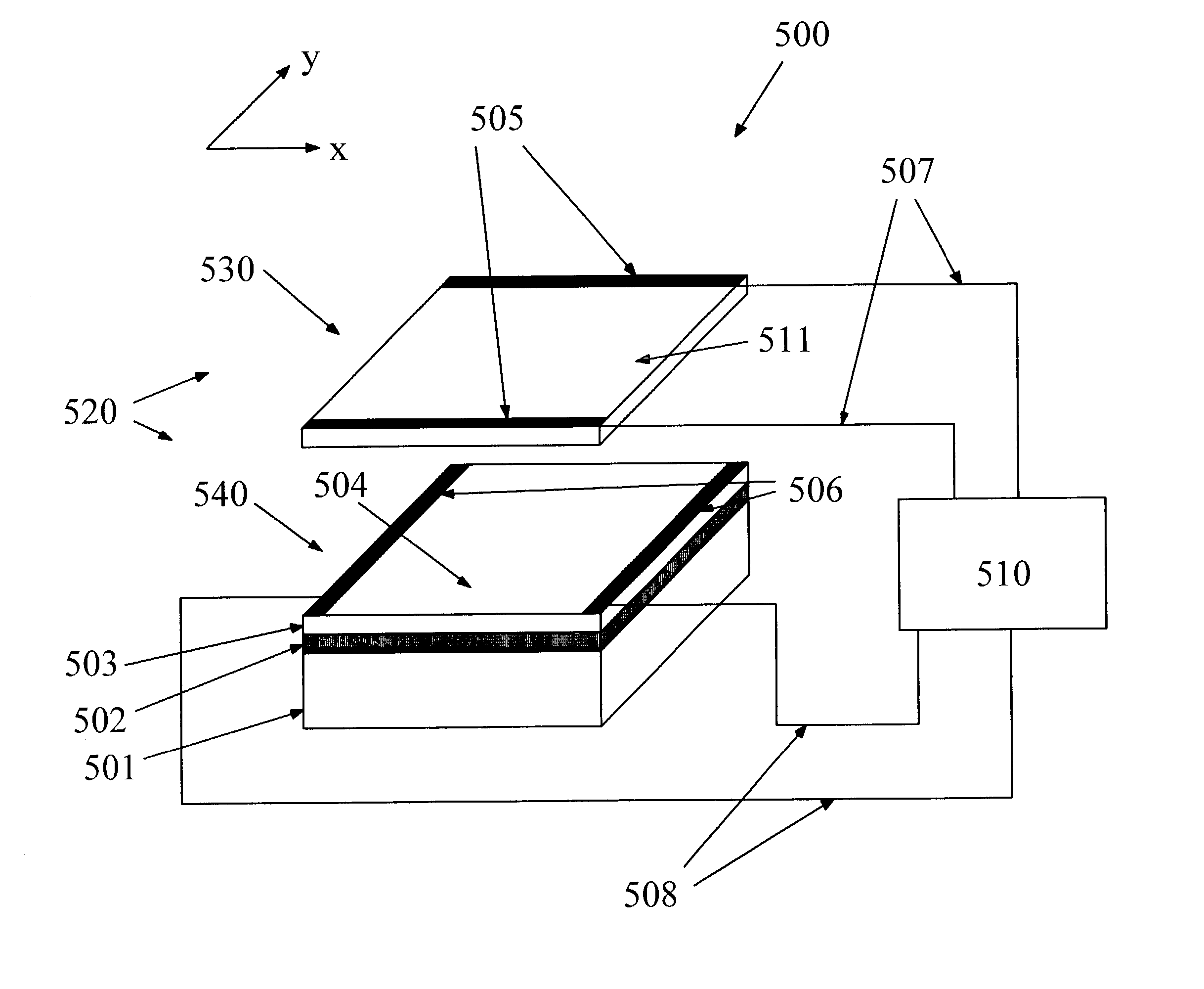
[0008]Generally, the present invention relates to touch sensors and touch sensing displays where it is desirable to have a set of desired properties with no or little trade off and where it is further desirable to reduce manufacturing cost.
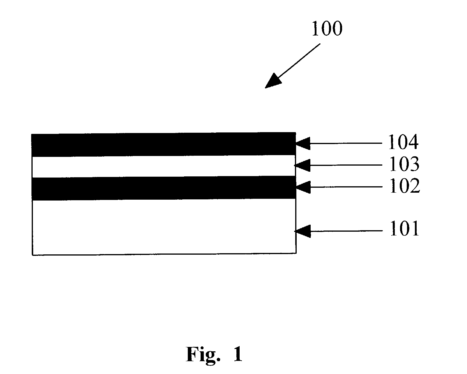
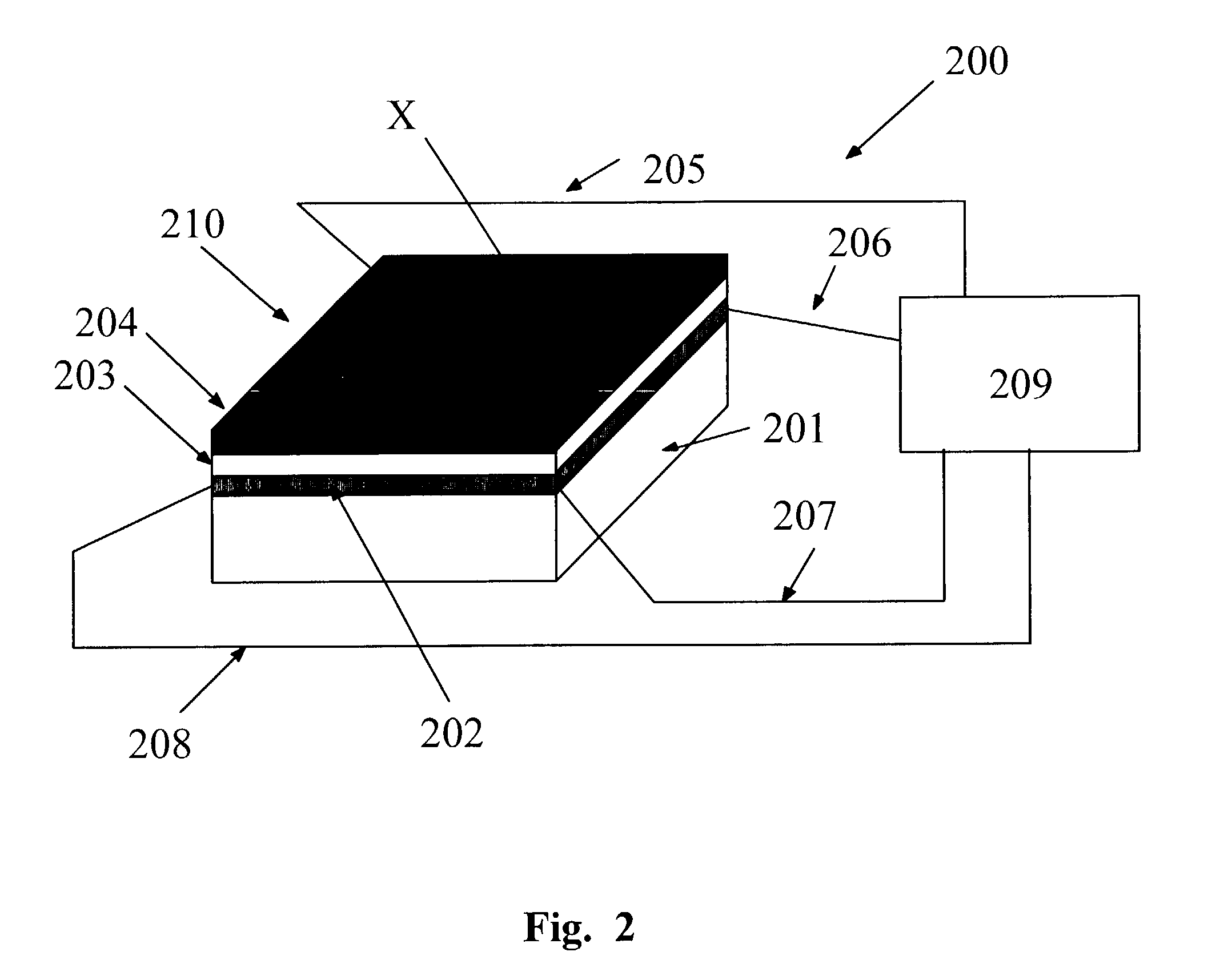
[0009]In one aspect of the invention a method of manufacturing a touch sensor component includes manufacturing a glass substrate followed by using atmospheric pressure chemical vapor deposition to deposit at least four films onto the glass substrate where the first film is designed primarily to have a desired optical clarity and sheet resistance, the second film is designed primarily to isolate the first film from the substrate, the third film is designed primarily to resist abrasion, and the fourth film is designed primarily to reduce glare.
[0013]In another aspect of the invention a touch sensitive display includes a float glass substrate and at least four films formed onto the glass substrate using an atmospheric pressure chemical vapor deposition technique where the first film is designed primarily for a pre-determined optical clarity and electrical conductivity, the second film is designed primarily for isolating the first film from the substrate, the third film is designed primarily for resisting abrasion, and the fourth film is designed primarily to reduce glare.

Problems solved by technology

Such specular reflection is generally referred to as glare and will reduce the viewability of the displayed information.
Generally, touch screens are susceptible to physical damage such as scratching.
Another characteristic of a touch screen is overall cost.
Generally, manufacturing cost increases as the number of layers in a touch screen is increased.
As one screen characteristic is improved, one or more other characteristics often degrade.

Method used


Image

  • Multifunctional multilayer optical film
  • Multifunctional multilayer optical film
  • Multifunctional multilayer optical film

Examples


Embodiment Construction

[0023]The present invention is generally applicable to touch screens, touch screens used with electronic display systems, and particularly where it is desirable for a touch screen to have high optical transmission, high contrast, high durability, low glare, low reflection, and low manufacturing cost. The present invention allows the optimization of a touch screen's desirable properties with no or little trade off. The present invention, furthermore, describes implementation of some of the listed desirable properties into a single layer, thereby further reducing design and manufacturing costs.

[0024]A touch screen can work on the general principle that an otherwise open electrical circuit is closed when a touch is applied. The properties of a signal generated in the closed circuit allows detection of a touch location. Different technologies may be employed to detect a touch location. One such technology is resistive. In a resistive touch, an applied touch brings two otherwise physical...


PUM

PropertyMeasurementUnit
Electrical conductoraaaaaaaaaa
Abrasion resistanceaaaaaaaaaa
Antireflectiveaaaaaaaaaa

Abstract

Optical component for use in a touch sensor and method of fabrication of same are disclosed. Optical component includes a multilayer optical film at least some layers of which are fabricated on the same manufacturing line and using the same manufacturing method. Each layer of the multilayer optical film is designed primarily to provide a desired associated property.

Description

FIELD OF THE INVENTION[0001]This invention generally relates to touch sensing devices. The invention is particularly applicable to such devices used in electronic display systems.BACKGROUND[0002]Touch screens allow a user to conveniently interface with an electronic display system by reducing or eliminating the need for a keyboard. For example, a user can carry out a complicated sequence of instructions by simply touching the screen at a location identified by a pre-programmed icon. The on-screen menu may be changed by re-programming the supporting software according to the application.[0003]Resistive and capacitive are two common touch sensing technologies. Both technologies typically incorporate one or more transparent conductive films as part of an electronic circuit that detects the location of a touch.[0004]The performance of a touch screen is described in terms of various characteristics of the screen. One such characteristic is optical transmission. Image brightness and contr...

Claims


Application Information

Patent Timeline
IPC IPC(8): G09G5/00C03C17/34G06F3/033G06F3/044G06F3/045
CPCC03C17/3417G06F3/045G06F3/044C03C17/3435G06F3/0445C03C17/34
Inventor SCHULZ, STEPHEN C.
Owner 3M INNOVATIVE PROPERTIES CO
Learn More