Centering mechanism, centering unit, semiconductor manufacturing apparatus, and centering method

a technology of semiconductor manufacturing apparatus and support table, which is applied in the direction of electrical programme control, program control, instruments, etc., can solve the problems of reducing production efficiency, affecting the efficiency of operation, and unable to carry the carrier around. , to achieve the effect of raising and lowering the support tabl

Inactive Publication Date: 2006-12-26
SAMSUNG ELECTRONICS CO LTD +1
View PDF15 Cites 10 Cited by
  • Summary
  • Abstract
  • Description
  • Claims
  • Application Information

AI Technical Summary

Benefits of technology

[0019](1) a lift mechanism to...

Problems solved by technology

If the diameter of each wafer is 300 mm or more, for example, the carrier that stores a plurality of wafers is so heavy that the operator can hardly carry the carrier around, which could be dangerous.
This problem is not limited to probers, and is common to semiconductor manufacturing apparatuses and other apparatuses that process wafer-type substrates.
If the wafers have large diameters or advanced hyperfine structures, processing each wafe...

Method used


Image

  • Centering mechanism, centering unit, semiconductor manufacturing apparatus, and centering method
  • Centering mechanism, centering unit, semiconductor manufacturing apparatus, and centering method
  • Centering mechanism, centering unit, semiconductor manufacturing apparatus, and centering method

Examples


Embodiment Construction

[0033]A centering mechanism, centering unit, and centering method for an object to be processed, according to the present invention, are applicable to any apparatuses that require centering of the object, besides a semiconductor manufacturing apparatus. To explain the invention specifically, the centering mechanism and the like that are used for a probe apparatus which checks devices on a wafer for electrical properties. Thus, the present invention is not limited to a probe apparatus.

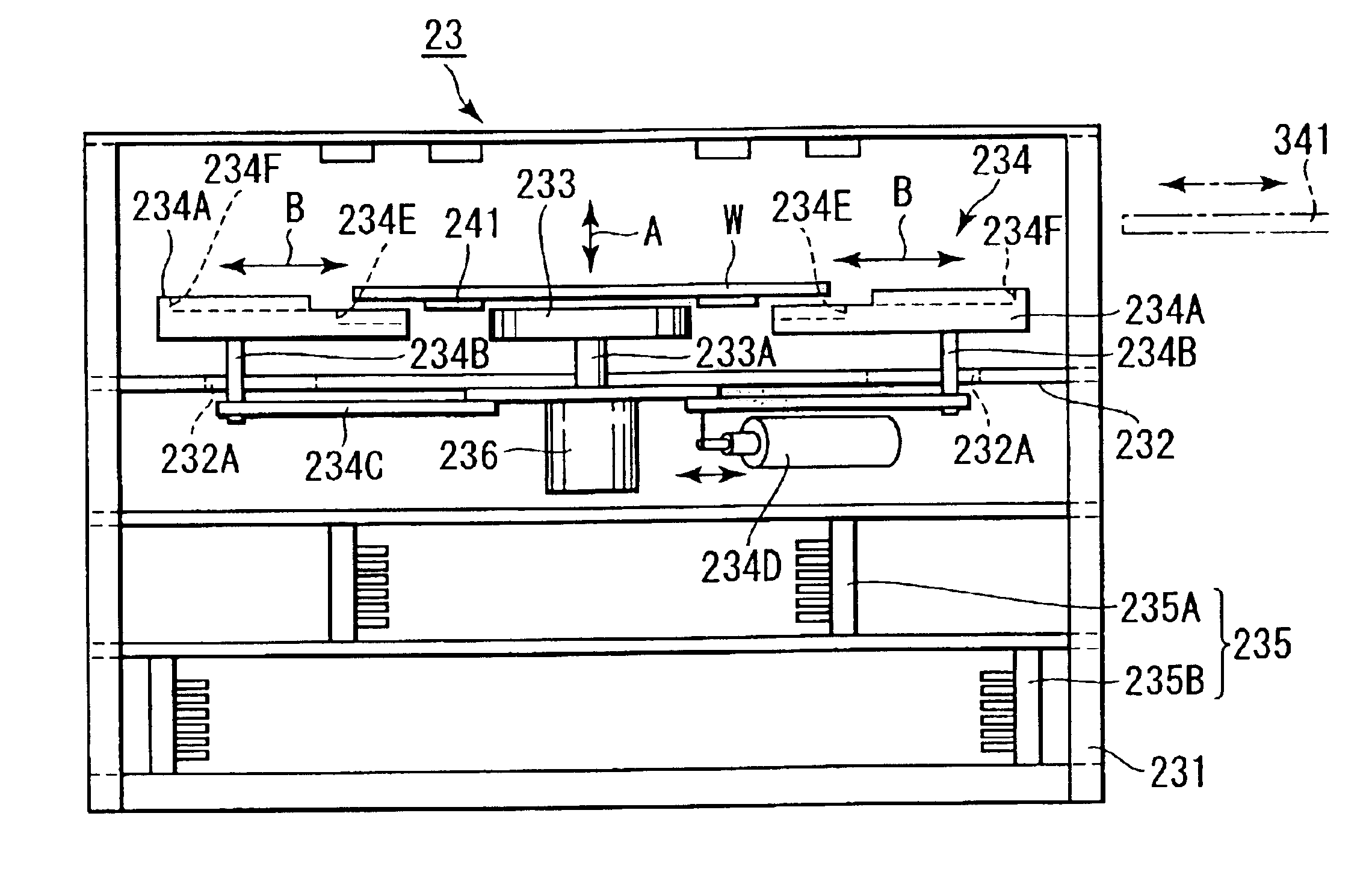
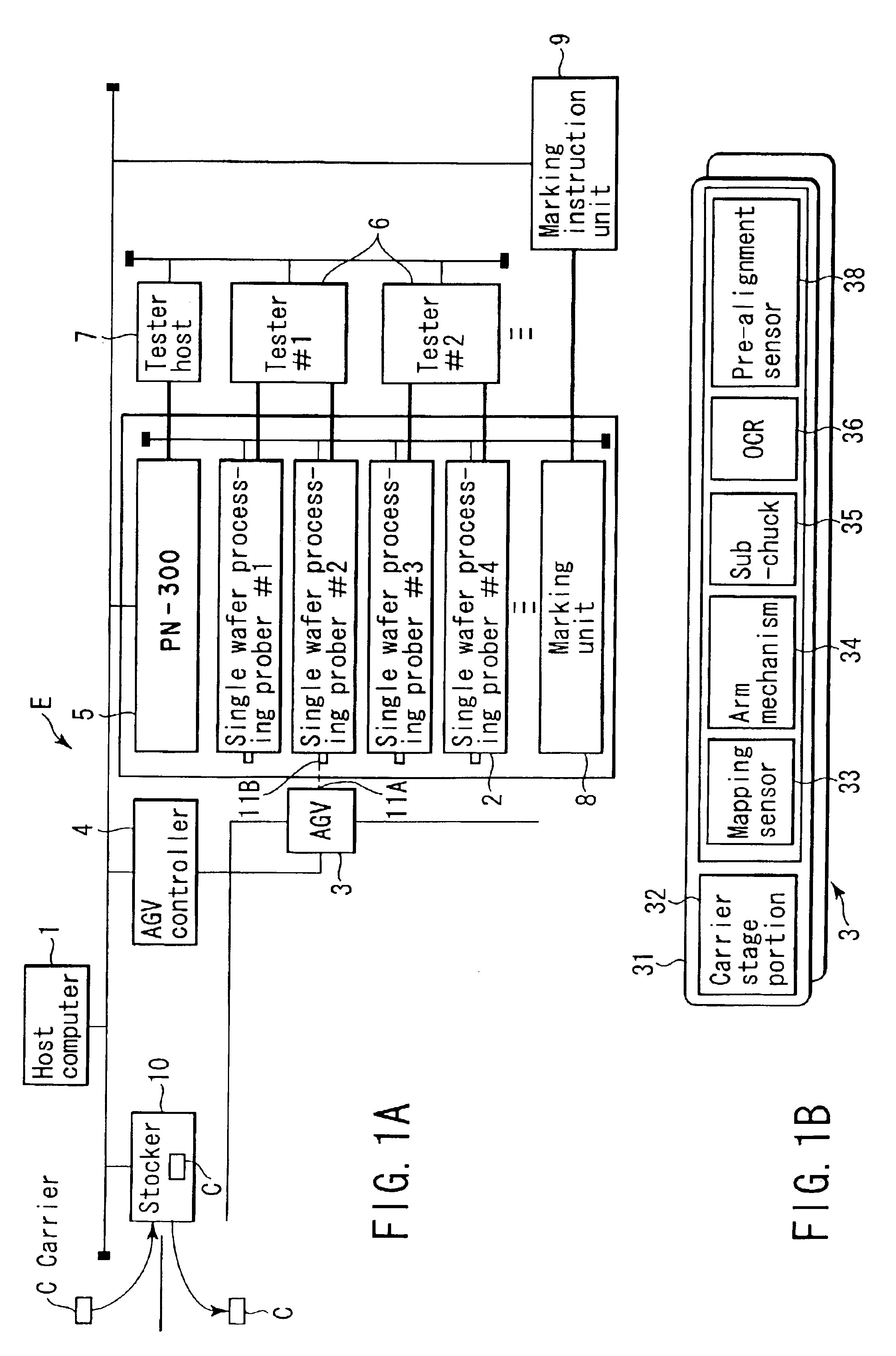
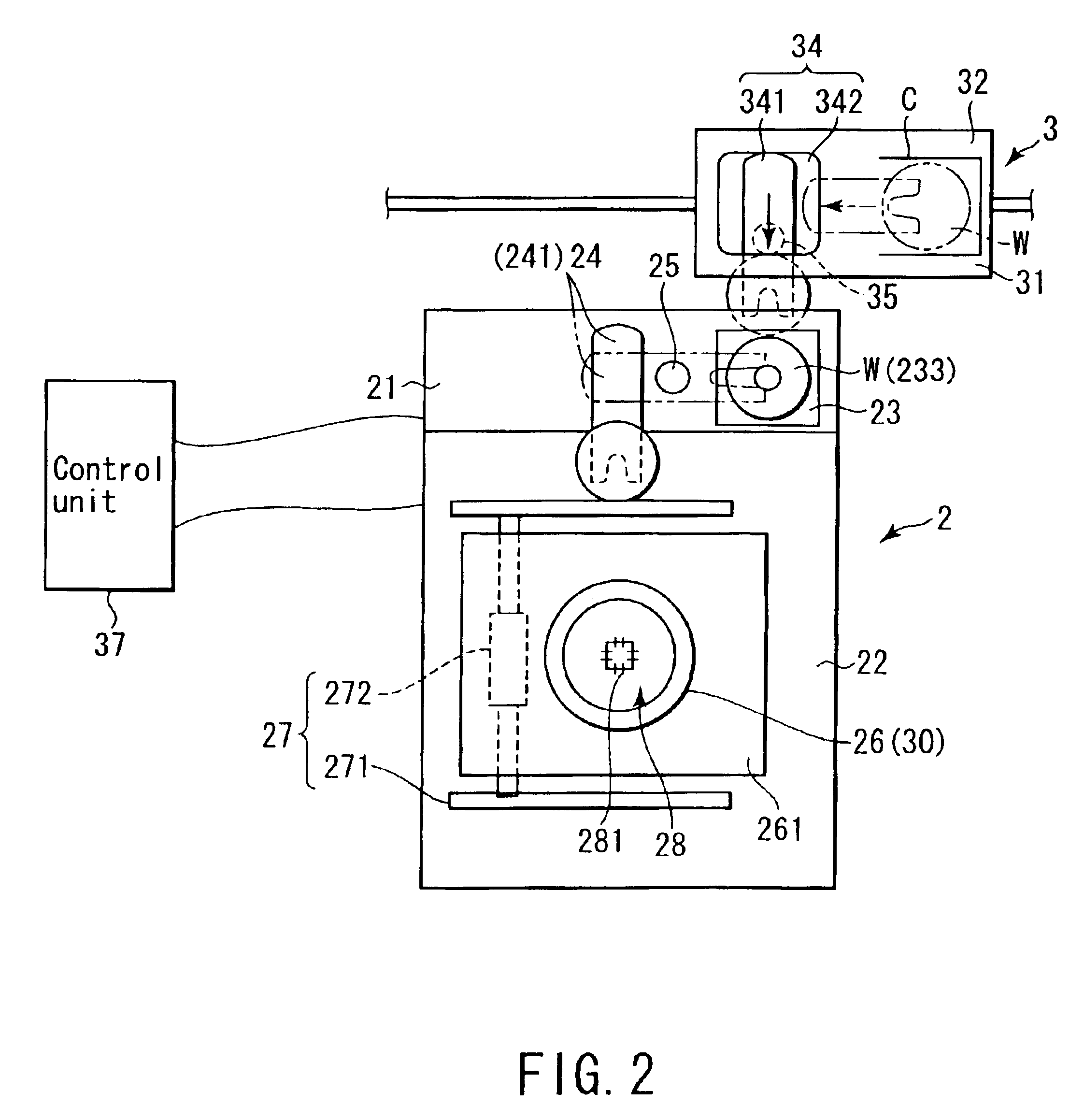
[0034]An embodiment of the invention will now be described with reference to FIGS. 1A to 4. The following is a description of a transportation system for an object to be processed (e.g., wafer) that can be applied to the centering unit and the semiconductor manufacturing apparatus of the invention. As shown in FIGS. 1A and 1B, this transportation system (automated material handling system (AMHS)) E may comprise a host computer 1, testing units (e.g., probers) 2, automated transportation devices (hereina...


PUM


Abstract

A centering unit comprises a plate, centering mechanism, link mechanism, and cylinder mechanism. The plate vertically divides the interior of a frame. The support table is located substantially on the center of the plate. The centering mechanism can center each wafer on the support table. Centering plates of the centering mechanism are located on either side of the support table and have engaging surfaces and that extend along the outer peripheral surface of the wafer. The link mechanism and the cylinder mechanism serve to extend and contract the space between the centering plates.

Description

CROSS-REFERENCE TO RELATED APPLICATIONS[0001]This application is based upon and claims the benefit of priority from the prior Japanese Patent Application No. 2002-018848, filed Jan. 28, 2002, the entire contents of which are incorporated herein by reference.BACKGROUND OF THE INVENTION[0002]1. Field of the Invention[0003]The present invention relates to a centering mechanism, centering unit, semiconductor manufacturing apparatus, and centering method, and more specifically, to a centering mechanism for securely delivering objects to be processed between an automated transportation device and a semiconductor manufacturing apparatus, a centering unit provided with the centering mechanism, a semiconductor manufacturing apparatus, and a centering method.[0004]2. Description of the Related Art[0005]In an inspection process of a semiconductor manufacturing apparatus, for example, probers are used as testing units for integrated circuits (hereinafter referred to as “devices”) that are forme...

Claims


Application Information

Patent Timeline
IPC IPC(8): B65G47/24H01L21/68H01L21/00H01L21/687
CPCH01L21/67259H01L21/68H01L21/68735Y10T279/26Y10S414/141Y10S414/136
Inventor KANG, KI SANGAKIYAMA, SHUJIHOSAKA, HIROKI
Owner SAMSUNG ELECTRONICS CO LTD
Why Eureka
Try Eureka