Semiconductor device, the method of manufacturing the same, and two-way switching device using the semiconductor devices

a semiconductor and semiconductor technology, applied in semiconductor devices, solid-state devices, transistors, etc., can solve the problems of high leakage current, short carrier generation lifetime, and large size of electric power converters, so as to facilitate the reduction of leakage current and reduce the on-voltage of igbt

a semiconductor and semiconductor technology, applied in semiconductor devices, solid-state devices, transistors, etc., can solve the problems of high leakage current, short carrier generation lifetime, and large size of electric power converters, so as to facilitate the reduction of leakage current and reduce the on-voltage of igbt

US7157785B2Inactive Publication Date: 2007-01-02FUJI ELECTRIC CO LTD

Image

  • Semiconductor device, the method of manufacturing the same, and two-way switching device using the semiconductor devices
  • Semiconductor device, the method of manufacturing the same, and two-way switching device using the semiconductor devices
  • Semiconductor device, the method of manufacturing the same, and two-way switching device using the semiconductor devices

Examples


second embodiment

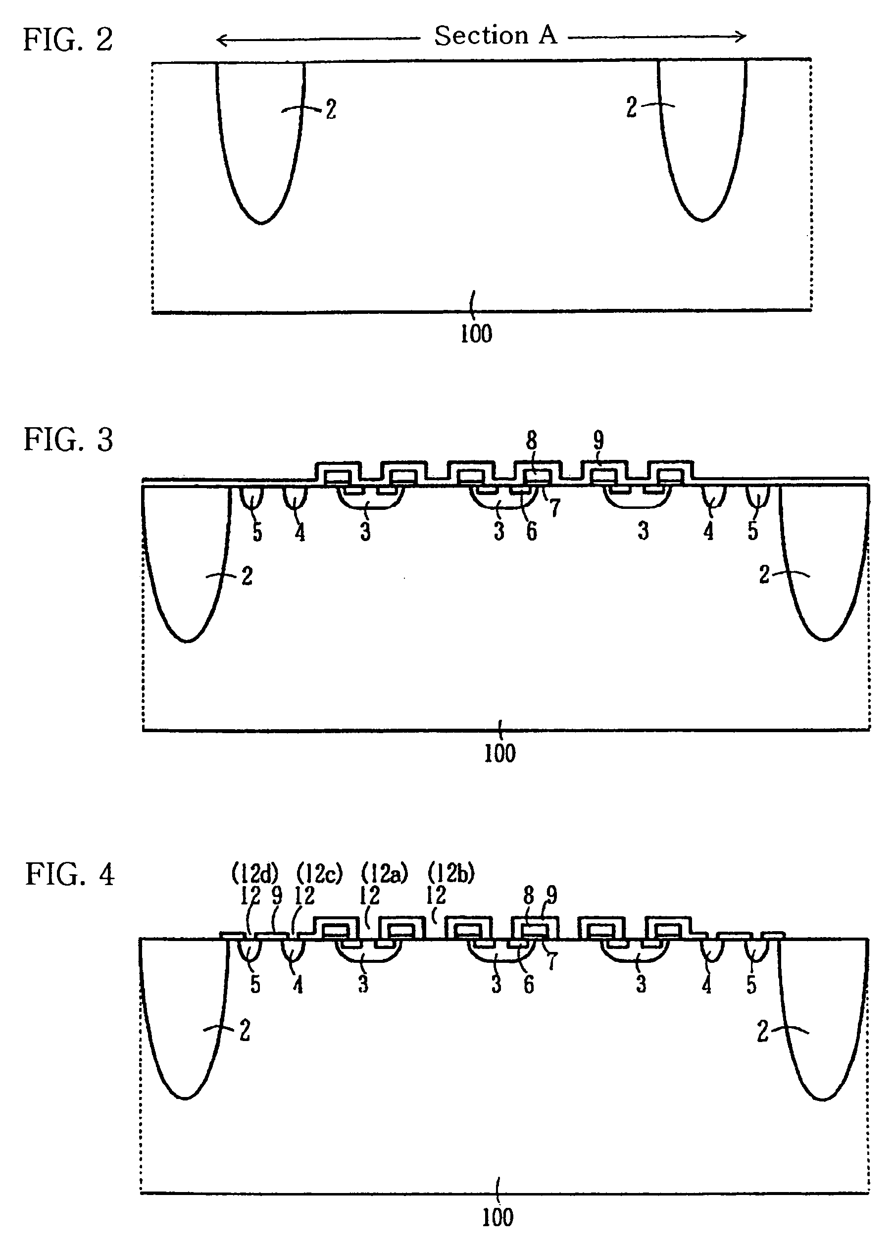
[0101]The IGBT is manufactured in the following way. Subsequent to the steps described with reference to FIGS. 2 through 4, boron ions are implanted at a low dose amount between 1×10¹¹ / cm2 and 1×10¹⁴ / cm2 and at a low acceleration voltage of 45 keV or lower. Then, emitter electrode 10 is formed by sputtering Al—Si1.0%. A metal with a high melting point such as titanium nitride and platinum silicide may be deposited before the above described sputtering. The Al—Si1.0% layer is sintered at 420° for 80 minutes (cf FIG. 5).

[0102]This sintering serves also as low-temperature activation for the lightly doped p-type bypass regions 17. Then, a surface protection film is coated on the semiconductor wafer and the back surface of the semiconductor wafer is lapped. A collector region is formed by ion implantation and subsequent annealing. Finally, the central portions of p+-type separation regions 2 are cut by dicing (cf FIG. 6) and a reverse blocking IGBT chip is completed. In the reverse bloc...

fifth embodiment

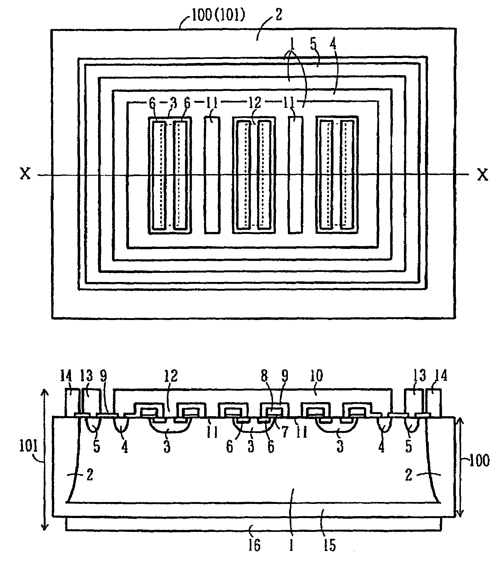
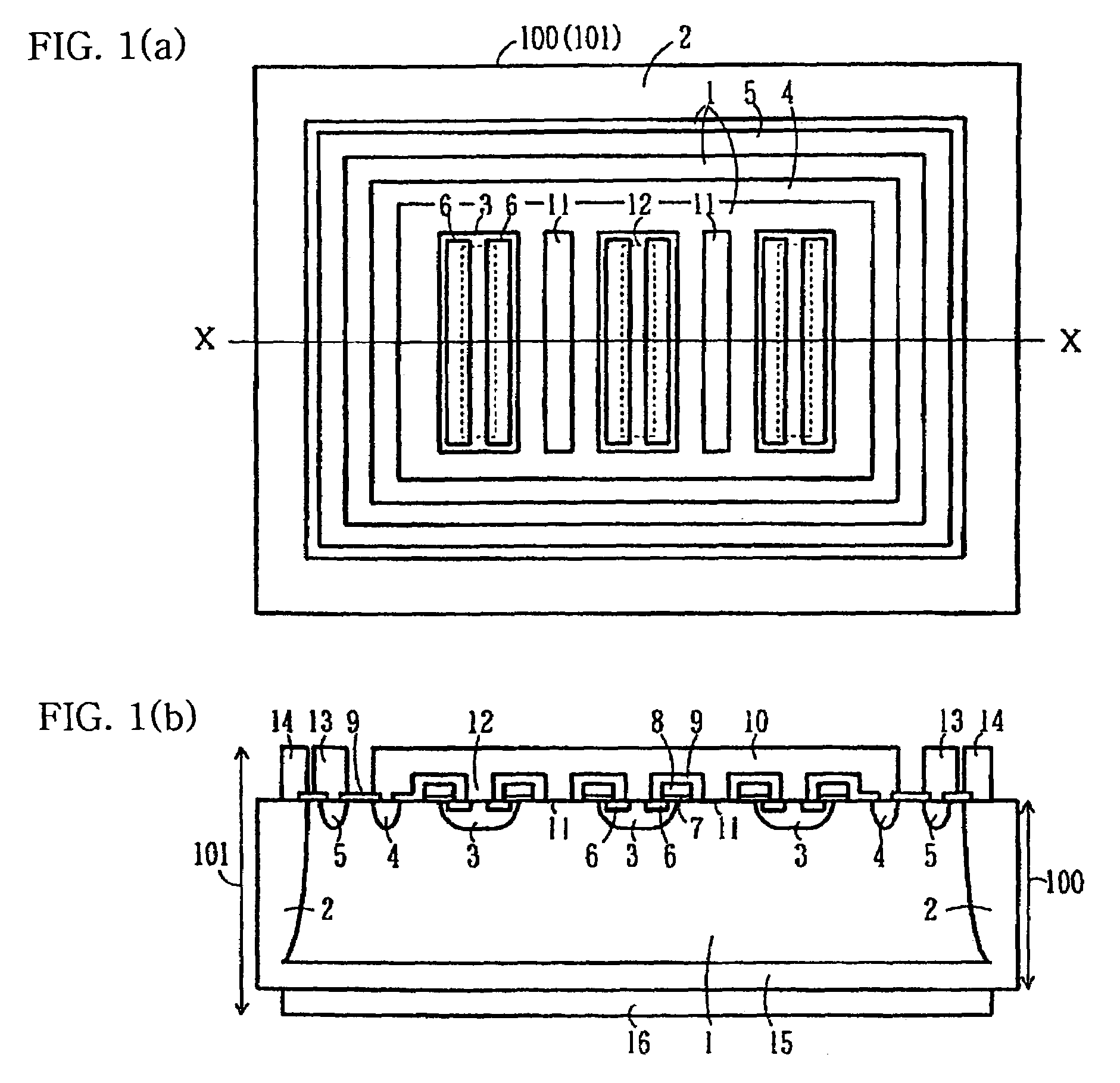
[0110]FIG. 11 is a top plan view of a semiconductor device according to the invention. In FIG. 11, Schottky junction 11 is shaped as an island and p-type base region 3 as a stripe. Since the area of Schottky junctions 11 in FIG. 11 is narrower than the area of Schottky junctions 11 in FIG. 1(a), the on-voltage of the IGBT in FIG. 11 is lower than the on-voltage of the IGBT in FIG. 1(a).

sixth embodiment

[0111]FIG. 12 is a top plan view of a semiconductor device according to the invention. In FIG. 12, Schottky junction 11 and p-type base region 3 are shaped as respective islands. In FIG. 12, the stripe-shaped p-type base regions 3 in FIG. 11 are replaced by island-shaped p-type base regions 3.

[0112]FIG. 13 is a top plan view of a semiconductor device according to a seventh embodiment of the invention. In FIG. 13, p-type bypass region 17 is shaped as an island and p-type base region 3 as a stripe. The semiconductor device according to a seventh embodiment is different from the semiconductor device according to the fifth embodiment shown in FIG. 11 in that Schottky junctions 11 in FIG. 11 are replaced by p-type bypass regions 17 in FIG. 13. The semiconductor device shown in FIG. 13 exhibits the same effects as those of the semiconductor device shown in FIG. 11.


PUM


Abstract

A semiconductor device is disclosed that reduces the reverse leakage current caused by reverse bias voltage application and reduces the on-voltage of the IGBT. A two-way switching device using the semiconductor devices is provided, and a method of manufacturing the semiconductor device is disclosed. The reverse blocking IGBT reduces the reverse leakage current and the on-voltage by bringing portions of an n−-type drift region 1 that extend between p-type base regions and an emitter electrode into Schottky contact to form Schottky junctions.

Description

CROSS REFERENCE TO RELATED APPLICATIONS[0001]This application claims priority from Japanese application Serial No. JP 2003-209709, filed on Aug. 29, 2003, and the contents of this document are incorporated herein by reference in their entirety.BACKGROUND OF THE INVENTION[0002]A. Field of the Invention[0003]The present invention relates to semiconductor devices such as power MOS devices used in electrical power converters. Specifically, the present invention relates to reverse blocking semiconductor devices exhibiting breakdown voltage characteristics (symmetrical or asymmetrical) including a forward breakdown voltage and a reverse breakdown voltage. The present invention relates also to the two-way switching devices using the reverse blocking semiconductor devices.[0004]B. Description of the Related Art[0005]VVVF inverters capable of varying the frequency and the voltage thereof are used very often to drive motors and such machines. Usually, the VVVF inverter includes a converter se...

Claims


Application Information

Patent Timeline
02 Jan 2007
Publication
US7157785B2
IPC
H01L27/102; H01L29/70; H01L31/07; H01L31/11; H01L29/06; H01L29/739; H01L29/872; H02M7/00
CPC
H01L29/0696; H02M7/003; H01L29/872; H01L29/7395
Inventors
TAKEI, MANABU; NAITO, TATSUYA