

Method of manufacturing a semiconductor film with little warp
a manufacturing method and technology of semiconductor film, applied in the direction of semiconductor devices, basic electric elements, electrical appliances, etc., can solve the problem of untreated substrate at a high temperature, and achieve the effect of reducing the warp
- Summary
- Abstract
- Description
- Claims
- Application Information
AI Technical Summary
Benefits of technology
Problems solved by technology
Method used
Image

Examples
embodiment mode 1
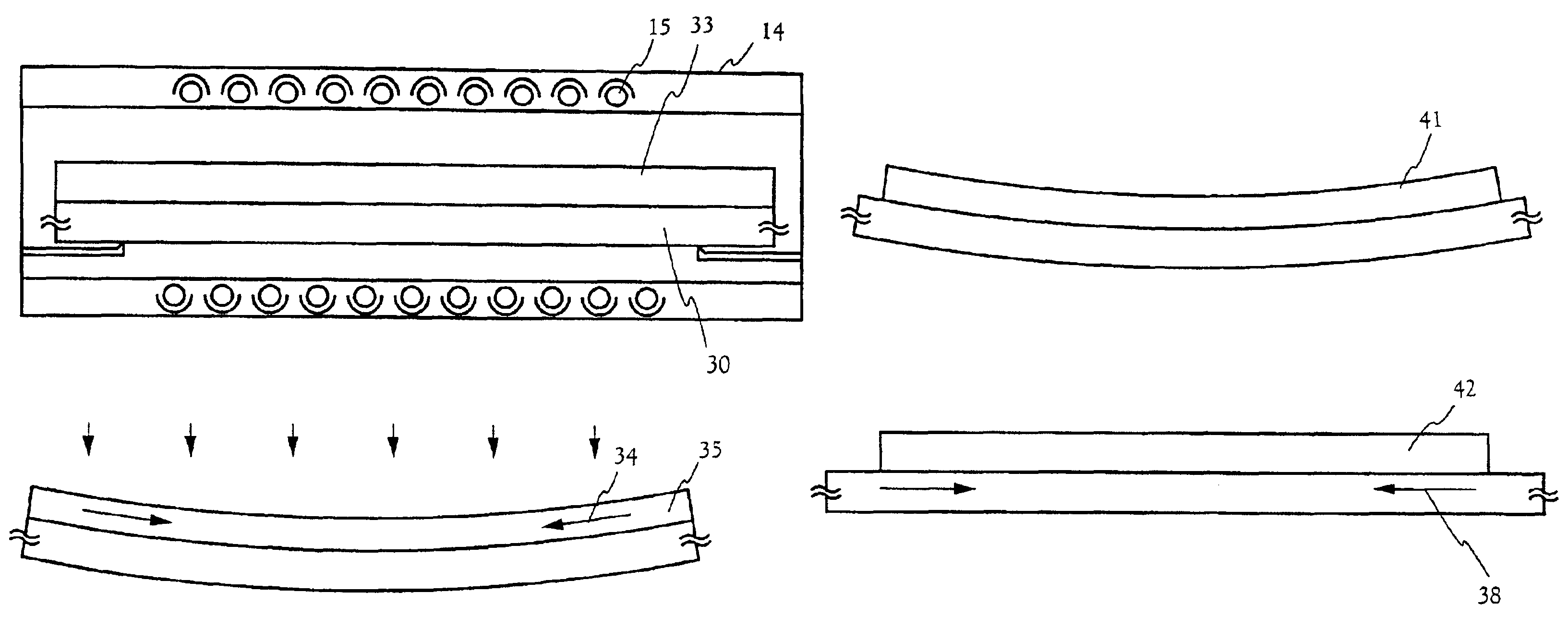
[Embodiment Mode 1]
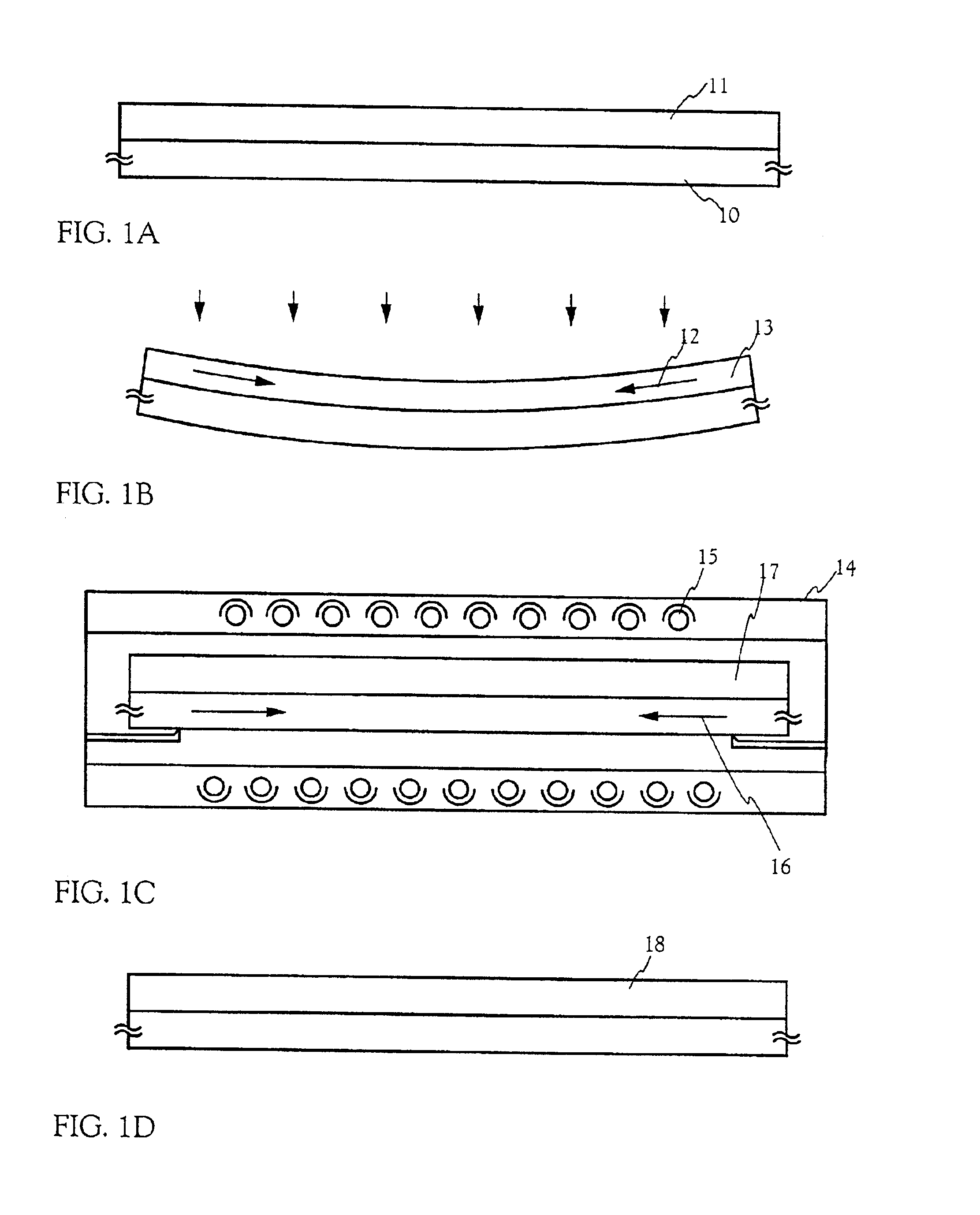
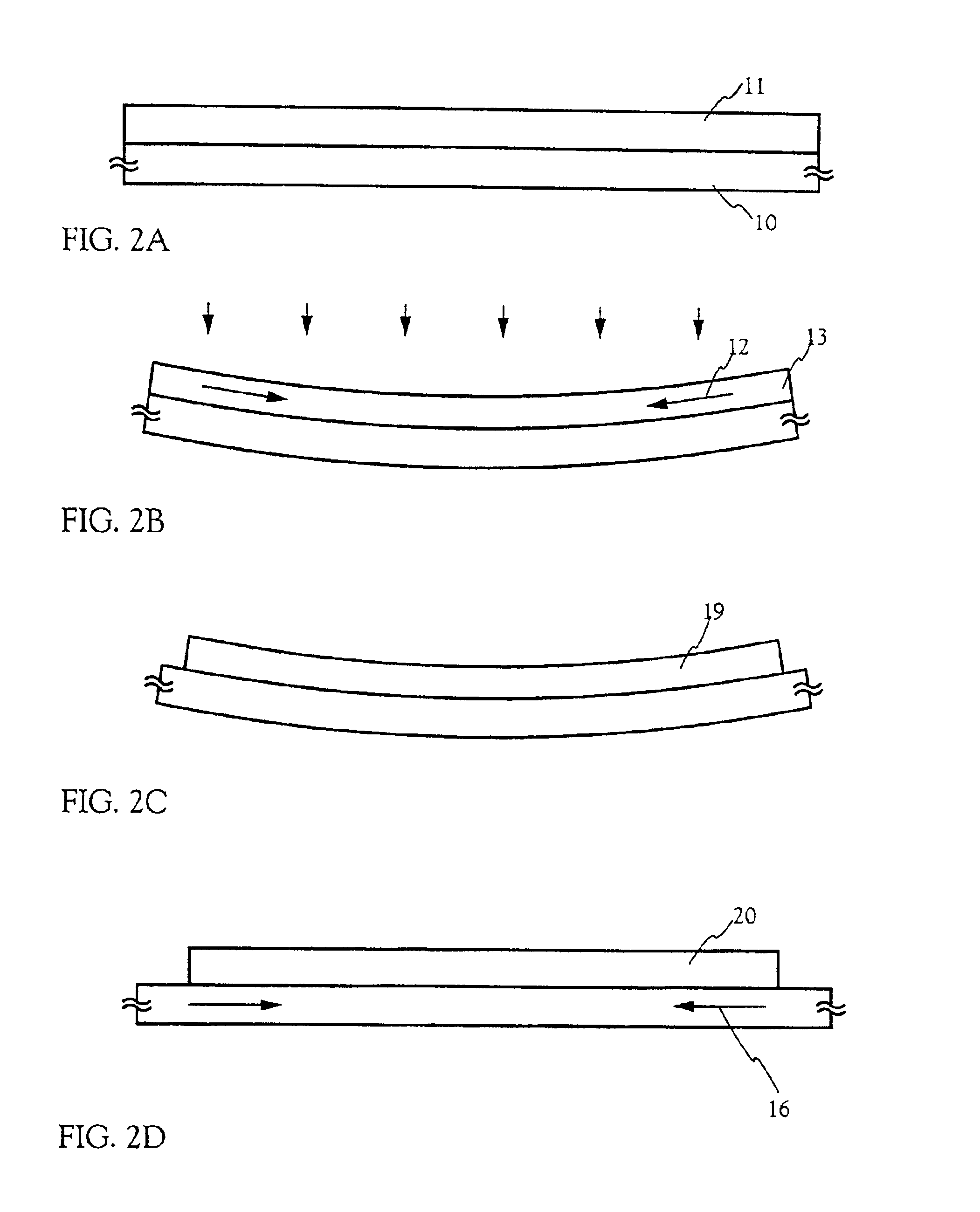
[0053]Embodiment Mode 1 of the present invention will be described with reference to FIGS. 1A to 1D.
[0054]First, a base insulating film (not shown) is formed on a substrate 10. A glass substrate or a quartz substrate having transmissivity is employed as the substrate 10. As the base insulating film, an insulating film such as a silicon oxide film, a silicon nitride film, or a silicon oxynitride film is formed. The structure of the base insulating film is not limited to a single layer. Lamination of at least two layers of the insulating films may also be employed. Further, the base insulating film may not be formed.
[0055]Next, a semiconductor film 11 is formed on the base insulating film. (FIG. 1A) The semiconductor film 11 is formed by depositing the amorphous semiconductor film using the well-known means such as a sputtering method, an LPCVD method or a plasma CVD method. The semiconductor film 11 is formed to have a thickness of 25 to 80 nm (preferably 30 to 60 ...
embodiment mode 2
[Embodiment Mode 2]
[0063]Embodiment Mode 2 of the present invention will be described with reference to FIGS. 20A to 20E.
[0064]First, the base insulating film (not shown) is formed on a substrate 30. The glass substrate or the quartz substrate having transmissivity is employed as the substrate 30. As the base insulating film, the insulating film such as the silicon oxide film, silicon nitride film, or silicon oxynitride film is formed. The structure of the base insulating film is not limited to a single layer. Lamination of at least two layers of the insulating films may also be employed. Further, the base insulating film may not be formed.
[0065]Next, a semiconductor film 31 is formed on the base insulating film. (FIG. 20A) The semiconductor film 31 is formed by depositing the amorphous semiconductor film using the well-known means such as the sputtering method, LPCVD method or plasma CVD method. The semiconductor film 31 is formed to have a thickness of 25 to 80 nm (preferably 30 t...
embodiment 1
[Embodiment 1]
[0076]Embodiment 1 of the present invention will be described with reference to FIGS. 1A to 1D.
[0077]First, the base insulating film (not shown) is formed on the substrate 10. The glass substrate or the quartz substrate having transmissivity is employed as the substrate 10. As the base insulating film, the insulating film such as the silicon oxide film, silicon nitride film, or silicon oxynitride film is formed. The structure of the base insulating film is not limited to a single layer. Lamination of at least two layers of the insulating films may also be employed. Further, the base insulating film may not be formed. In this embodiment, the glass substrate is employed, and the silicon oxynitride film (not shown) having a film thickness of 150 nm is formed on the glass substrate by the plasma CVD method.
[0078]Next, the semiconductor film 11 is formed on the base insulating film. (FIG. 1A) The semiconductor film 11 is formed by depositing the amorphous semiconductor film...
PUM
 Abstract
Description
Claims
Application Information