Liquid crystal display unit and method for driving the same
a technology of liquid crystal display and display unit, which is applied in the direction of static indicating device, cathode-ray tube indicator, instruments, etc., can solve the problems of insufficient writing, reduced on-screen contrast, and general response of liquid crystal, so as to reduce in-plane brightness difference and flicker, high brightness, and high contrast
- Summary
- Abstract
- Description
- Claims
- Application Information
AI Technical Summary
Benefits of technology
Problems solved by technology
Method used
Image
Examples
second embodiment
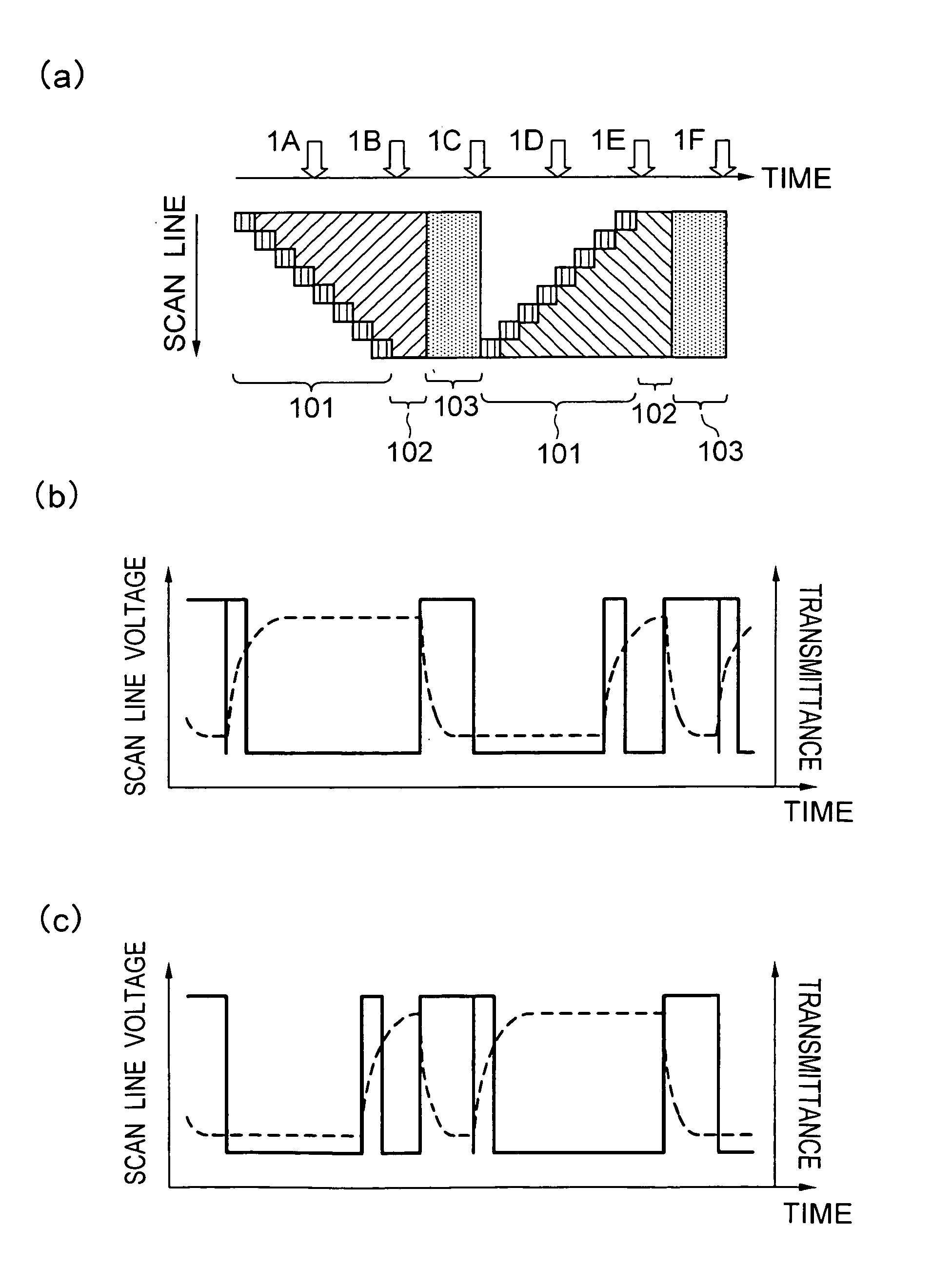
[0095]FIGS. 12(a)–12(c) are time charts that show a second embodiment of the present invention in the same manner as in FIGS. 10(a)–10(c). In the present embodiment, bi-directional scanning is performed as in the first embodiment. However, the present embodiment differs from the first embodiment in that the position of the reset period is changed from that in the first embodiment, and interlace drive is employed. In the present embodiment, one half of the eight scan lines (odd-numbered scan lines, hereinafter called “odd scan lines”) are scanned (selected) in the first field, and the remaining half of the eight scan lines (even-numbered scan lines, hereinafter called “even scan lines”) are scanned (selected) in the second field. The reset period 103 for each scan line is positioned at the end of the field in which the scan line is not scanned (selected). Specifically, for odd scan lines, a write period 101 is provided in the first field such that these scan lines are successively sc...
third embodiment
[0099]FIGS. 14(a)–14(c) are time charts that show a third embodiment of the present invention in the same manner as in FIGS. 10(a)–10(c). In the present embodiment, bi-directional scanning is performed in combination with interlace drive as in the second embodiment. The method for driving of the present embodiment can be achieved through modification of the method for driving of the second embodiment such that the frame frequency is doubled. That is, as shown in FIG. 10(a), for odd scan lines, a write period 101 is provided in a first half of the first field such that these scan lines are successively scanned from the top for write operation, followed by a display period 102. A reset period 103 is provided at the end of the first field. The second field is similarly divided into these periods. By contrast, for even scan lines, a reset period 103 is provided at the end of the first half of the first field, a write period 101 is provided in the second half of the first field such that...
fourth embodiment
[0102]FIGS. 16(a)–16(c) are time charts that show a fourth embodiment in the same manner as in FIGS. 10(a)–10(c). In the present embodiment, bi-directional scanning is performed in combination with interlace drive as in the second and third embodiments. However, the present embodiment differs from the second and third embodiments in that the interlace drive is performed within each of the first and second fields, but the scanning direction in the second field is opposite to that in the first field. That is, for odd scan lines, a write period 101 is provided in a first half of the first field such that these scan lines are successively scanned from the top, followed by a display period 102, and a reset period 103 is provided at the end of the first field. Subsequently, a write period 101 is provided in a first half of the second field such that these scan lines are successively scanned from the bottom, followed by a display period 102, and a reset period 103 is provided at the end of...
PUM
| Property | Measurement | Unit |
|---|---|---|
| time | aaaaa | aaaaa |
| time | aaaaa | aaaaa |
| time period | aaaaa | aaaaa |
Abstract
Description
Claims
Application Information


