Layer capacitor element and production process as well as electronic device

a production process and capacitor technology, applied in the field of capacitors, can solve the problems of reducing the performance of the capacitor, reducing the characteristics, and reducing the dielectric material, and achieve the effect of excellent high-frequency tracking performance and low characteristic deterioration

Inactive Publication Date: 2007-01-09
FUJITSU LTD
View PDF16 Cites 52 Cited by
  • Summary
  • Abstract
  • Description
  • Claims
  • Application Information

AI Technical Summary

Benefits of technology

[0034]It is therefore an object of the present invention to provide a thin layer capacitor element which solves the problems related to reduction of the dielectric material which occurs when a resin material such as polyimide is used as a protective insulating layer to absorb the mechanical stress from bumps, and which has excellent high-frequency tracking performance and low deterioration of characteristics.
[0035]It is another object of the invention to increase an adhesion strength between a substrate such as a semiconductor substrate and a capacitor, particularly a lower electrode of the capacitor element, while limiting the number of sputtering apparatuses required for fabrication and to thereby keep the production costs to a minimum.
[0036]In addition to the above objects, the object of the invention is to provide a thin layer capacitor element which undergoes no deterioration in characteristics by water generated during resin curing for formation of the protective layer and which therefore requires no barrier layer.

Problems solved by technology

However, as the miniature size and the large capacity of a thin layer capacitor is achieved by using a metal oxide as the dielectric material, the metal oxide undergoes reduction during the fabrication process and thereby produces deterioration in the characteristics.
Such a solution, however, results in the following new problems.
As the first problem, there is the problem of reduction of the dielectric material in the step of forming the protective insulating layer.
This occurs because the H2O infiltrates the capacitor electrodes in a hydrogen ion state due to the catalytic effect of the platinum Pt composing the electrodes, and the hydrogen ions reach the interface between the electrodes and the dielectric material by diffusion, thereby resulting in oxygen loss of the dielectric material.
The second problem is a problem which occurs during actual use in the field, though this is not a problem of the production steps illustrated in the prior art process.
This problem occurs due to the moisture absorption property of the resin material whereby, due to the high temperature surrounding the thin layer capacitor, moisture in the air absorbed by the polyimide resin migrates to the internal capacitor at a high temperature and reduces the dielectric material.
In addition to the above problems, the conventional production processes suffer from other problems.
However, thin layer capacitor elements produced in this manner are often exposed to a reducing atmosphere in the solder reflow step or undergo absorption of water or moisture from the external environment, leading to problems such as deterioration of the electrical characteristics of the dielectric substance and short-circuiting between the upper electrode layer and lower electrode layer.
Particularly when platinum (Pt) is used as the electrode material, Pt readily allows penetration of hydrogen, a problem which is exacerbated by generation of hydrogen due to the catalytic effect on water.
The prior art protective layers mentioned above have been effective for capacitor elements incorporated into semiconductor devices such as FRAMs, but in cases where flip chip connections are created with solder bumps as stand-alone capacitors, no alleviation in the stress from the solder bumps can be expect d and therefore it has not been possible to completely eliminate the problem of deterioration in the characteristics.
However, the water generated by the above protective layer-forming reaction can cause a major problem in that it impairs the characteristics of the obtained thin layer capacitor element.
When water contacts the electrode layer, the catalytic effect of the Pt promotes infiltration of the hydrogen atoms of the water into the electrode layer, producing an oxygen deficiency in the dielectric oxide at the interface between the dielectric layer and the electrode layer.

Method used


Image

  • Layer capacitor element and production process as well as electronic device
  • Layer capacitor element and production process as well as electronic device
  • Layer capacitor element and production process as well as electronic device

Examples


example 1

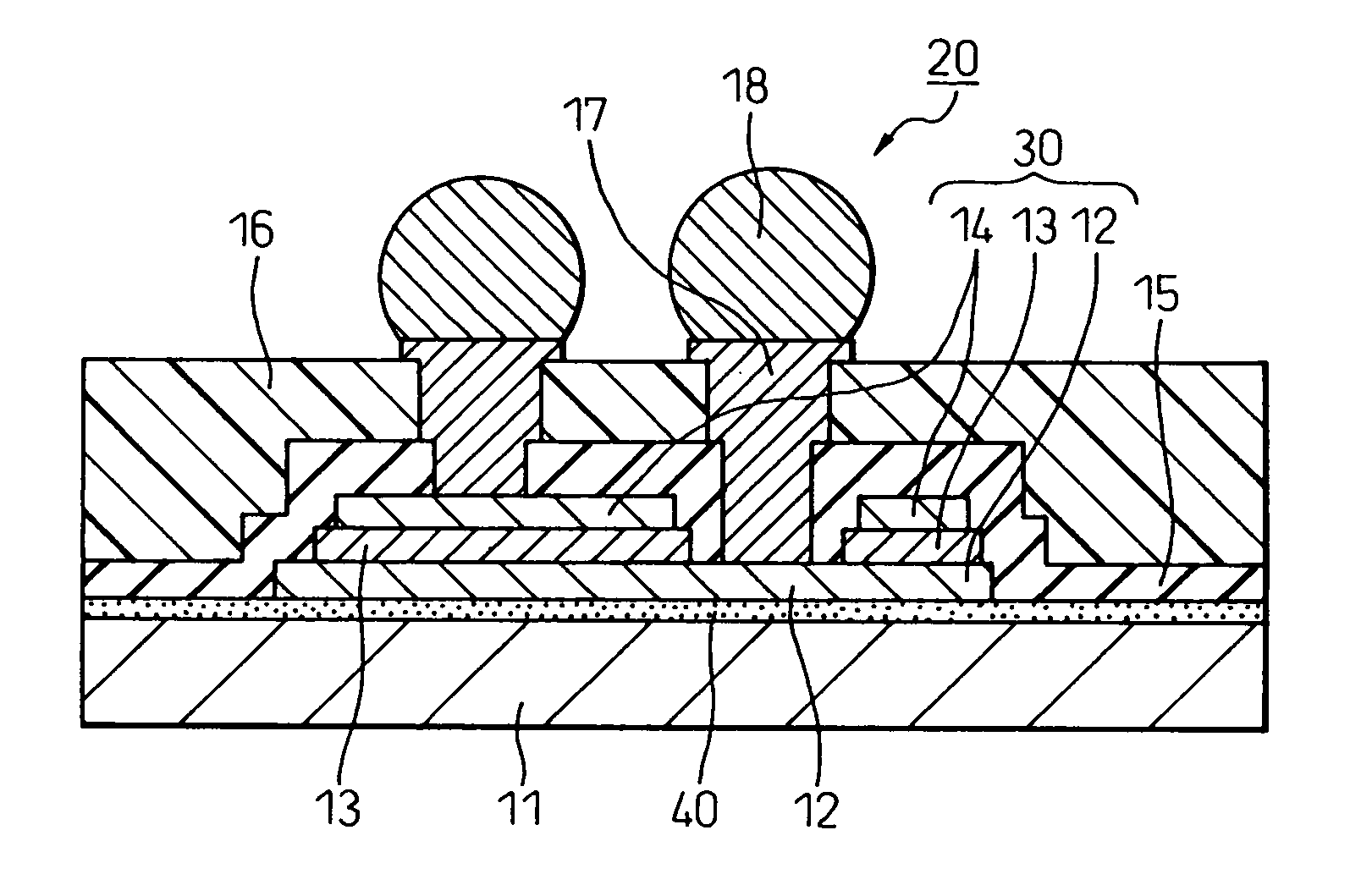
[0321]In this example, a thin layer capacitor element was produced having the layer structure explained above with reference to FIG. 16. Specifically, the thin layer capacitor element of this example is provided with a capacitor structure comprising a lower electrode layer, dielectric layer and upper electrode layer, on a silicon substrate produced upon fabrication of a silicon wafer, and the top side of the capacitor structure is covered with a protective insulating layer according to the invention.

[0322]After thermal oxidation of the silicon substrate to form a silicon oxide film (SiO2) on the surface, RF magnetron sputtering was carried out to form a TiO2 adhesion layer with a thickness of 20 nm on the SiO2 film. The sputtering conditions for the TiO2 layer were a substrate temperature of 500° C., an RF power of 200 W, a gas pressure of 0.1 Pa and an Ar / O2 ratio of 7 / 2.

[0323]Next, a platinum (Pt) film was formed by DC magnetron sputtering to form the lower electrode layer. A lowe...

example 2

[0332]The procedure described in Example 1 was repeated but, for this example, benzocyclobutene (BCB) resin was used as the protective insulating layer in place of an epoxy resin.

[0333]RF magnetron sputtering was carried out to form a TiO2 adhesive layer with a thickness of 20 nm on the SiO2 film formed on the silicon substrate.

[0334]Next, a platinum (Pt) film was formed by DC magnetron sputtering to form the lower electrode layer having a thickness of 100 nm. Further, in this example, for the reference, the lower electrode layer and an upper electrode layer described below were also formed from iridium (Ir) in place of Pt. The characteristics of the resulting thin layer capacitor element using Ir were satisfactory comparable to those obtained using Pt.

[0335]After forming the lower electrode layer, barium strontium titanate (Ba0.7Sr0.3)TiO3 (BST) was used as the starting material to form a dielectric layer by RF magnetron sputtering. The BST film sputtering conditions were a substra...


PUM

PropertyMeasurementUnit
areaaaaaaaaaaa
temperatureaaaaaaaaaa
thicknessaaaaaaaaaa

Abstract

In one aspect of the invention, in a thin layer capacitor element comprising a capacitor having a dielectric layer made of a metal oxide and a protective insulating layer made of a resin material, a barrier layer made of a non-conductive inorganic material is provided between the capacitor and the protective insulating layer. In another aspect of the invention, a thin layer capacitor element is constituted so that a capacitor structure is covered with at least one protective insulating layer composed of a cured resin, the cured resin being formed from at least one resin precursor selected from the group consisting of thermosetting resins, photosetting resins and thermoplastic resins.

Description

CROSS-REFERENCE TO RELATED APPLICATIONS[0001]This application is based upon and claims the benefit of priorities from the prior Japanese Patent Applications Nos.: 2002-330578, filed Nov. 14, 2002; 2003-63558, filed Mar. 10, 2003; and 2003-94732, filed Mar. 31, 2003; the entire contents of which are incorporated herein by reference.BACKGROUND OF THE INVENTION[0002]1. Field of the Invention[0003]The present invention relates to a capacitor and, specifically, it relates to a thin layer capacitor element comprising a capacitor formed on a substrate, such as a semiconductor substrate, by a thin layer fabrication process. More particularly, the present invention relates to a thin layer capacitor element provided with a barrier layer, between a capacitor and a protective insulating layer, to inhibit a reduction of the metal oxide dielectric layer by moisture from the protective insulating layer. Further, the present invention relates to a thin layer capacitor element provided with an impro...

Claims


Application Information

Patent Timeline
Patent Type & Authority Patents(United States)
IPC IPC(8): H01G4/228H01G4/06H01G4/33H01L21/02H01L23/31H01L23/522H01L27/08
CPCH01G4/228H01G4/33H01L23/3114H01L23/5223H01L27/0805H01L28/57H01L28/65H01L2924/00013H01L2924/3011H01L2924/19041H01L2224/13022H01L2224/131H01L2224/16H01L2924/01046H01L2924/01077H01L2924/01078H01L2924/01079H01L2924/04941H01L2924/014H01L2224/13099H01L2224/05023H01L2224/05001H01L2224/05647H01L2924/00014H01L2224/05655H01L2224/05666H01L2224/05671H01L2224/05166H01L2224/05169
Inventor KURIHARA, KAZUAKISHIOGA, TAKESHIBANIECKI, JOHN DAVIDKURASHINA, MAMORU
Owner FUJITSU LTD
Why Eureka
Try Eureka