Layer capacitor element and production process as well as electronic device

a production process and capacitor technology, applied in the field of capacitors, can solve the problems of reducing the performance of the capacitor, reducing the characteristics, and reducing the dielectric material, and achieve the effect of excellent high-frequency tracking performance and low characteristic deterioration

Inactive Publication Date: 2006-11-09
FUJITSU LTD
View PDF8 Cites 20 Cited by
  • Summary
  • Abstract
  • Description
  • Claims
  • Application Information

AI Technical Summary

Benefits of technology

[0033] It is therefore an object of the present invention to provide a thin layer capacitor element which solves the problems related to reduction of the dielectric material which occurs when a resin material such as polyimide is used as a protective insulating layer to absorb the mechanical stress from bumps, and which has excellent high-frequency tracking performance and low deterioration of characteristics.
[0034] It is another object of the invention to increase an adhesion strength between a substrate such as a semiconductor substrate and a capacitor, particularly a lower electrode of the capacitor element, while limiting the number of sputtering apparatuses required for fabrication and to thereby keep the production costs to a minimum.
[0035] In addition to the above objects, the object of the invention is to provide a thin layer capacitor element which undergoes no deterioration in characteristics by water generated during resin curing for formation of the protective layer and which therefore requires no barrier layer.

Problems solved by technology

However, as the miniature size and the large capacity of a thin layer capacitor is achieved by using a metal oxide as the dielectric material, the metal oxide undergoes reduction during the fabrication process and thereby produces deterioration in the characteristics.
Such a solution, however, results in the following new problems.
As the first problem, there is the problem of reduction of the dielectric material in the step of forming the protective insulating layer.
This occurs because the H2O infiltrates the capacitor electrodes in a hydrogen ion state due to the catalytic effect of the platinum Pt composing the electrodes, and the hydrogen ions reach the interface between the electrodes and the dielectric material by diffusion, thereby resulting in oxygen loss of the dielectric material.
The second problem is a problem which occurs during actual use in the field, though this is not a problem of the production steps illustrated in the prior art process.
This problem occurs due to the moisture absorption property of the resin material whereby, due to the high temperature surrounding the thin layer capacitor, moisture in the air absorbed by the polyimide resin migrates to the internal capacitor at a high temperature and reduces the dielectric material.
In addition to the above problems, the conventional production processes suffer from other problems.
However, thin layer capacitor elements produced in this manner are often exposed to a reducing atmosphere in the solder reflow step or undergo absorption of water or moisture from the external environment, leading to problems such as deterioration of the electrical characteristics of the dielectric substance and short-circuiting between the upper electrode layer and lower electrode layer.
Particularly when platinum (Pt) is used as the electrode material, Pt readily allows penetration of hydrogen, a problem which is exacerbated by generation of hydrogen due to the catalytic effect on water.
The prior art protective layers mentioned above have been effective for capacitor elements incorporated into semiconductor devices such as FRAMs, but in cases where flip chip connections are created with solder bumps as stand-alone capacitors, no alleviation in the stress from the solder bumps can be expected and therefore it has not been possible to completely eliminate the problem of deterioration in the characteristics.
However, the water generated by the above protective layer-forming reaction can cause a major problem in that it impairs the characteristics of the obtained thin layer capacitor element.
When water contacts the electrode layer, the catalytic effect of the Pt promotes infiltration of the hydrogen atoms of the water into the electrode layer, producing an oxygen deficiency in the dielectric oxide at the interface between the dielectric layer and the electrode layer.

Method used


Image

  • Layer capacitor element and production process as well as electronic device
  • Layer capacitor element and production process as well as electronic device
  • Layer capacitor element and production process as well as electronic device

Examples


first embodiment

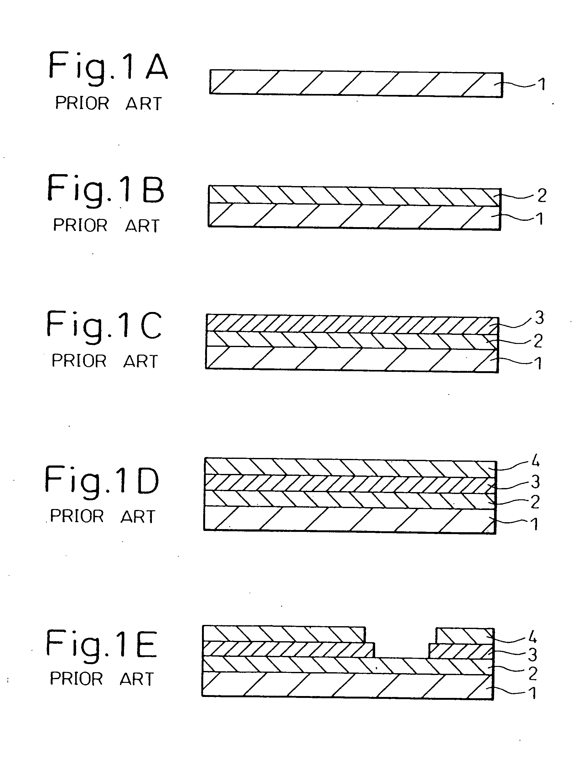
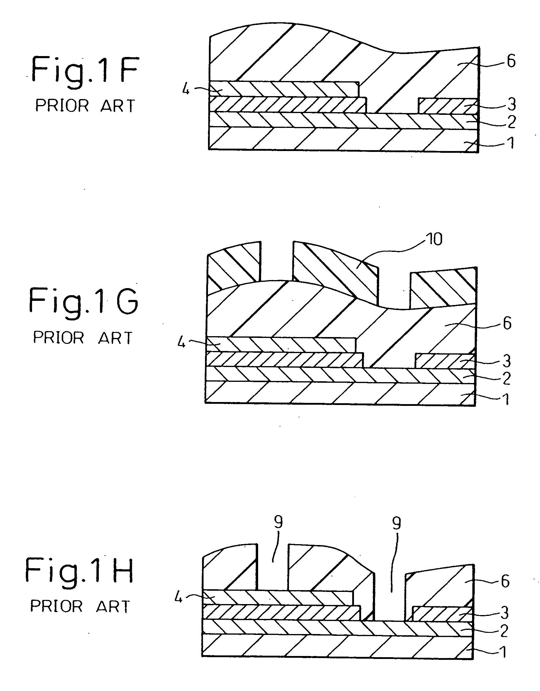
[0098] A thin layer capacitor element according to a first embodiment of the present invention will now be explained with reference to FIG. 5 and FIGS. 6A to 6J showing, in sequence the production process of the thin layer capacitor element.

[0099] (1) Capacitor-Forming Step

[0100] As shown in FIGS. 6A to 6D, a lower electrode layer 12 composed of platinum, a dielectric layer 13 composed of a composite oxide and an upper electrode layer 14 composed of platinum Pt are formed in that order on a silicon substrate 11 prepared as the supporting substrate, to form a capacitor 30 which is also referred herein to as a “capacitor structure”.

[0101] A metal oxide (such as BST) with a high dielectric constant is used herein as the material for the dielectric layer 13 to achieve downsizing and large capacitance.

[0102] Further, a precious metal such as platinum (Pt) or iridium (Ir), having excellent oxidation resistance in high temperature environments and allowing satisfactory crystal orientat...

second embodiment

[0152] A process for production of a thin layer capacitor element according to a second embodiment of the invention will now be explained.

[0153] The production process according to this embodiment can be carried out in accordance with the manner which is the same as that of the first embodiment described above with reference to FIGS. 6A to 6J. However, in this embodiment, formation of the dielectric layer 13 shown in FIG. 6C is carried out using a sputtering method in place of a sol-gel method, in contrast to the first embodiment. Also, a BST material in an amorphous state having the same composition as that of the dielectric layer 13 is used as the barrier layer 15 for the step of forming the barrier layer 15 shown in FIG. 6F.

[0154] First, a silicon wafer is used as the silicon substrate 11, and a sputtering method is used to form films of titanium oxide (TiO2; 20 nm) and platinum (Pt; 100 nm) in that order on the silicon wafer, as shown in FIGS. 6A to 6D, in the same manner as t...

third embodiment

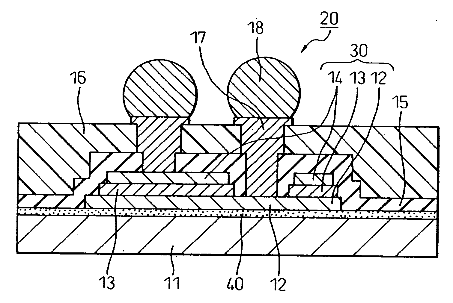
[0163] A thin layer capacitor element according to a third embodiment of the invention will now be explained with reference to FIGS. 10 and 11, in which FIG. 10 is a perspective view of a thin layer capacitor element, and FIG. 11 is a cross-sectional view taken along line XI-XI of FIG. 10.

[0164] This embodiment is an application example of the thin layer capacitor element according to the first embodiment, and as shown in FIG. 10, a plurality of bumps are arrayed as terminals for the thin layer capacitor element 20 on one side of the thin layer capacitor element 20. The plurality of bumps 18 are arranged such that adjacent bumps are connected to different electrodes of the capacitor (capacitor structure) 30.

[0165] Specifically, each bump is electrically connected to every other electrode, and the connected capacitors 30 are internally connected together, as shown in FIG. 11.

[0166] For external connection of each bump, a bump 18a is connected to the power line of a circuit board (...


PUM

PropertyMeasurementUnit
areaaaaaaaaaaa
temperatureaaaaaaaaaa
thicknessaaaaaaaaaa

Abstract

In one aspect of the invention, in a thin layer capacitor element comprising a capacitor having a dielectric layer made of a metal oxide and a protective insulating layer made of a resin material, a barrier layer made of a non-conductive inorganic material is provided between the capacitor and the protective insulating layer. In another aspect of the invention, a thin layer capacitor element is constituted so that a capacitor structure is covered with at least one protective insulating layer composed of a cured resin, the cured resin being formed from at least one resin precursor selected from the group consisting of thermosetting resins, photosetting resins and thermoplastic resins.

Description

[0001] This application is a divisional of U.S. application Ser. No. 10 / 706,288, filed Nov. 13, 2003.CROSS-REFERENCE TO RELATED APPLICATIONS [0002] This application is based upon and claims the benefit of priorities from the prior Japanese Patent Applications Nos.: 2002-330578, filed Nov. 14, 2002; 2003-63558, filed Mar. 10, 2003; and 2003-94732, filed Mar. 31, 2003; the entire contents of which are incorporated herein by reference. BACKGROUND OF THE INVENTION [0003] 1. Field of the Invention [0004] The present invention relates to a capacitor and, specifically, it relates to a thin layer capacitor element comprising a capacitor formed on a substrate, such as a semiconductor substrate, by a thin layer fabrication process. More particularly, the present invention relates to a thin layer capacitor element provided with a barrier layer, between a capacitor and a protective insulating layer, to inhibit a reduction of the metal oxide dielectric layer by moisture from the protective insul...

Claims


Application Information

Patent Timeline
Patent Type & Authority Applications(United States)
IPC IPC(8): H01G4/228H01G4/06H01G4/33H01L21/02H01L23/31H01L23/522H01L27/08
CPCH01G4/228H01G4/33H01L2924/00013H01L2924/3011H01L2924/19041H01L23/3114H01L23/5223H01L27/0805H01L28/57H01L28/65H01L2224/13022H01L2224/131H01L2224/16H01L2924/01046H01L2924/01077H01L2924/01078H01L2924/01079H01L2924/04941H01L2924/014H01L2224/13099H01L2224/05001H01L2224/05023H01L2224/05647H01L2924/00014H01L2224/05655H01L2224/05666H01L2224/05671H01L2224/05166H01L2224/05169
Inventor KURIHARA, KAZUAKISHIOGA, TAKESHIBANIECKI, JOHN DAVIDKURASHINA, MAMORU
Owner FUJITSU LTD
Why Eureka
Try Eureka