Semiconductor die package with reduced inductance and reduced die attach flow out

a technology of inductance reduction and die package, which is applied in the field of semiconductor device packaging, can solve the problems of extremely limited reduction of achieve the effects of reducing the inductance, and reducing the length of the bond wir

Inactive Publication Date: 2007-01-16
SKYWORKS SOLUTIONS INC
View PDF33 Cites 15 Cited by
  • Summary
  • Abstract
  • Description
  • Claims
  • Application Information

AI Technical Summary

Benefits of technology

[0013]According to various embodiments of the invention, greater control of die attach adhesive flow out during semiconductor packaging is achieved and, as a result, length of bond wires can be reduced, which leads to reduced inductance. Furthermore, package size

Problems solved by technology

However, due to a number of factors, the amount of reduction th

Method used


Image

  • Semiconductor die package with reduced inductance and reduced die attach flow out
  • Semiconductor die package with reduced inductance and reduced die attach flow out
  • Semiconductor die package with reduced inductance and reduced die attach flow out

Examples


Embodiment Construction

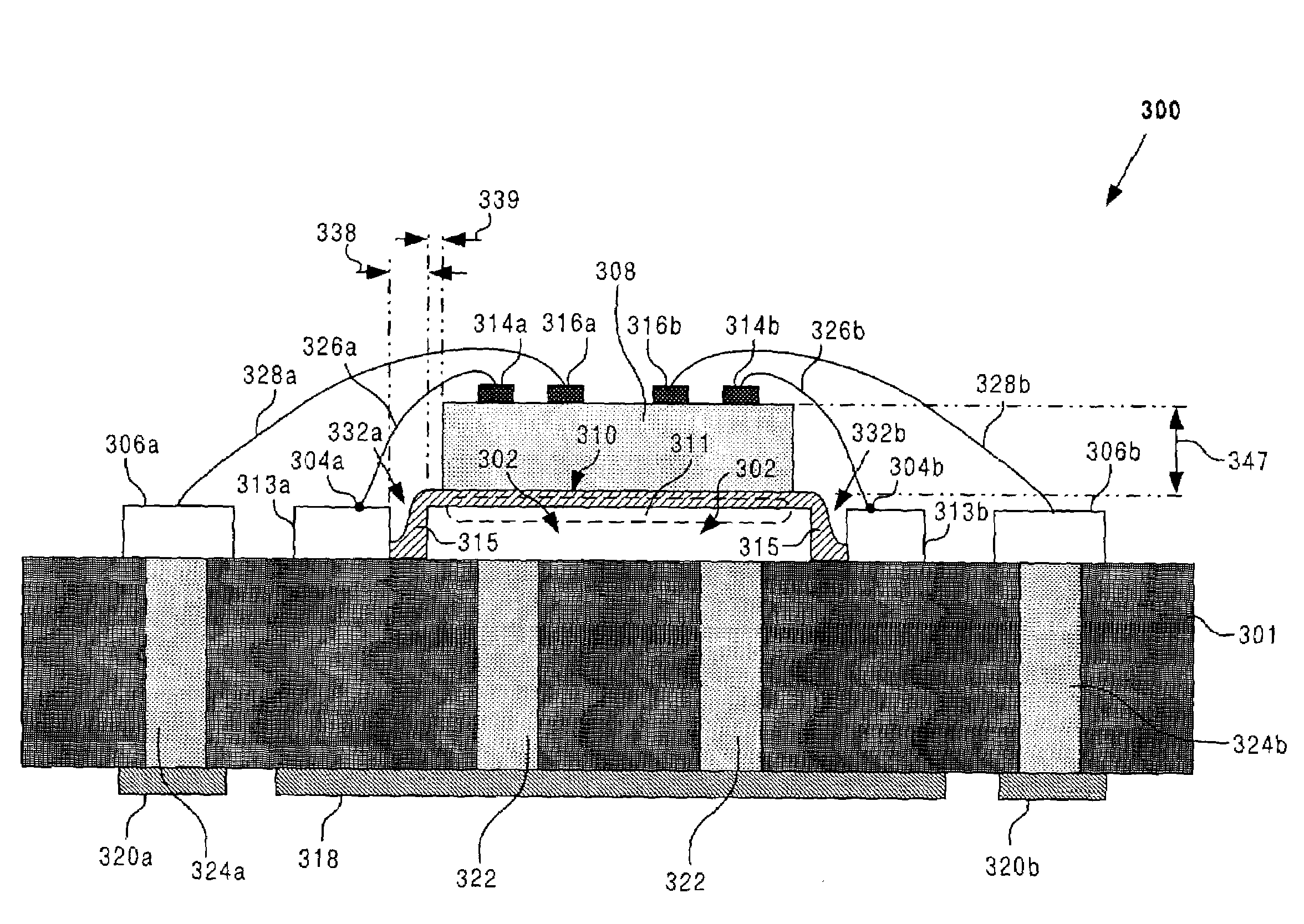
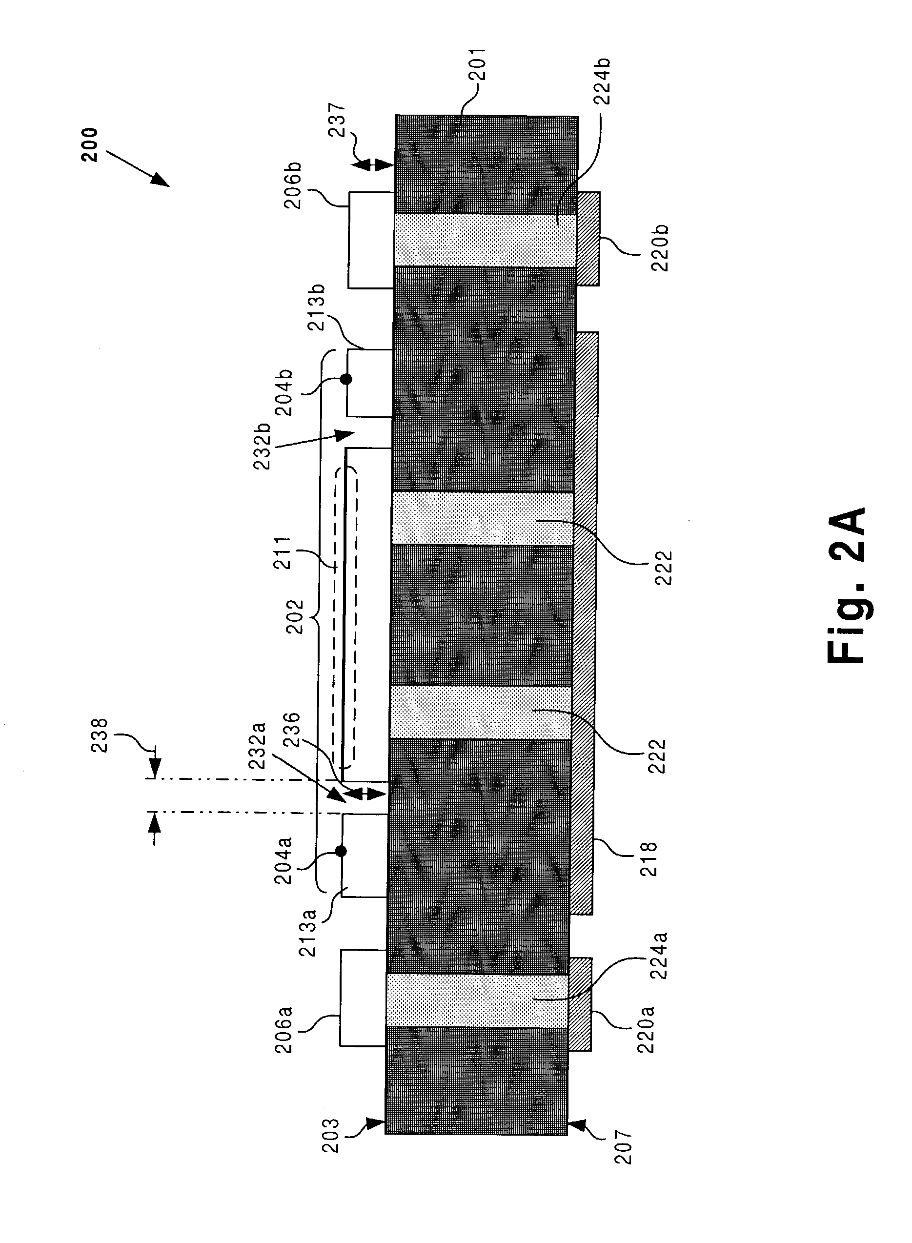
[0019]The present invention is directed to a semiconductor die package with reduced inductance and reduced die attach adhesive flow out. The following description contains specific information pertaining to the implementation of the present invention. One skilled in the art will recognize that the present invention may be implemented in a manner different from that specifically discussed in the present application. Moreover, some of the specific details of the invention are not discussed in order to not obscure the invention. The specific details not described in the present application are within the knowledge of a person of ordinary skill in the art.

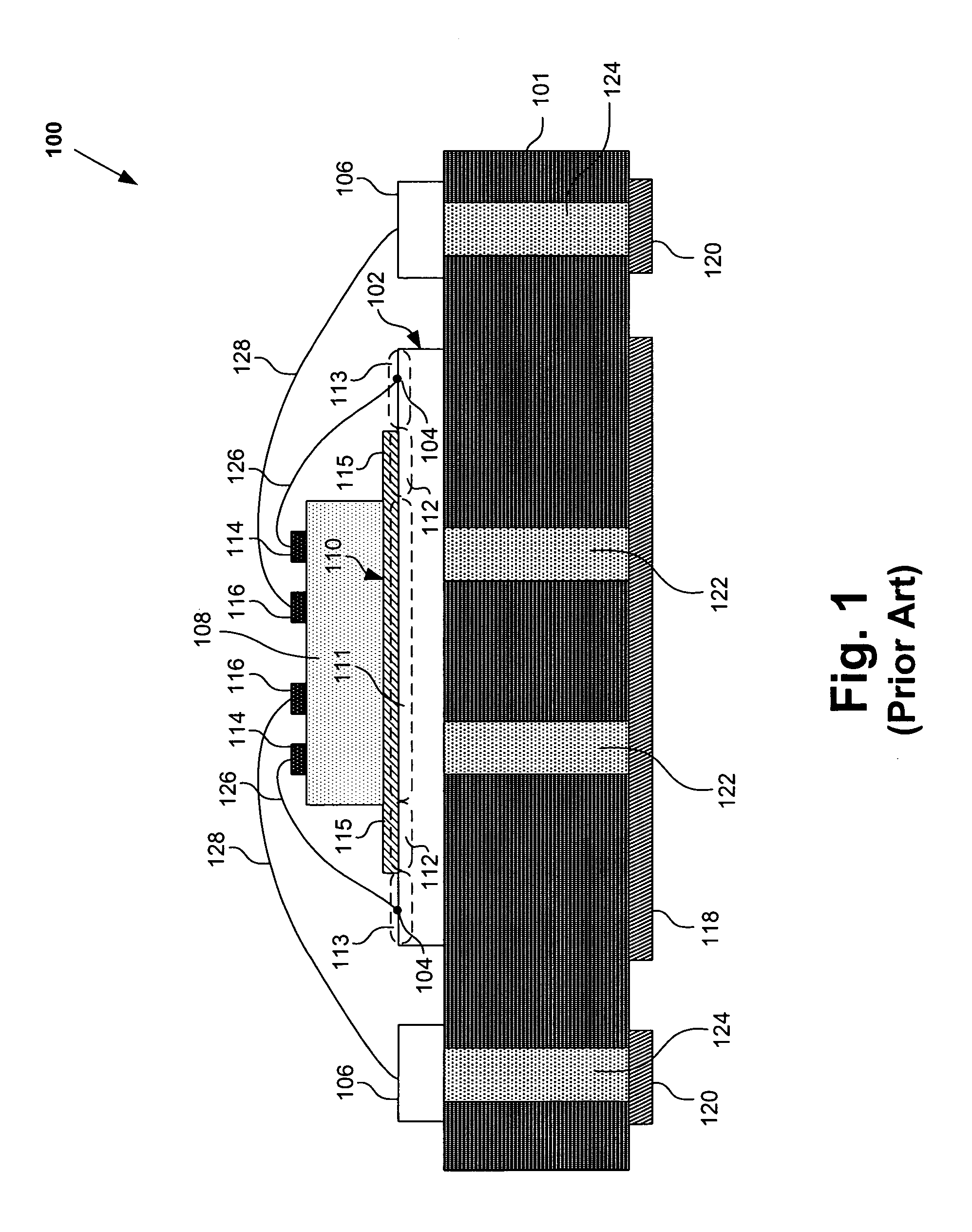
[0020]The drawings in the present application and their accompanying detailed description are directed to merely exemplary embodiments of the invention. To maintain brevity, other embodiments of the invention which use the principles of the present invention are not specifically described in the present application and are not specific...


PUM


Abstract

In one exemplary embodiment, a structure comprises a substrate having a top surface, and a die attach pad situated on the top surface of the substrate. The die attach pad includes a die attach region and at least one substrate ground pad region electrically connected to the die attach region. The die attach pad further includes a die attach stop between the die attach region and the at least one substrate ground pad region. The die attach stop acts to control and limit die attach adhesive flow out to the at least one substrate ground pad region during packaging so that the at least one substrate ground pad region can be moved closer to die attach region so that shorter bond wires for connecting the at least one substrate ground pad region to a die wire bond pad may be used during packaging.

Description

BACKGROUND OF THE INVENTION[0001]1. Field of the Invention[0002]The present invention is generally in the field of semiconductors. More specifically, the invention is in the field of semiconductor packaging.[0003]2. Related Art[0004]During semiconductor packaging, dice are mounted onto a die attach pad fabricated on a substrate surface. A die adhesive is commonly used to attach the die to the die attach pad. For example, epoxy resin is a common type of die attach adhesive used for this purpose. Such epoxies can be referred to as “die attach epoxies.” After the die is mounted on the substrate, bond wires are used to electrically connect die wire bond pads located on the die to their corresponding substrate ground pads and substrate signal pads located on the substrate.[0005]In general, it is desirable to reduce the length of the bond wires used to connect the die wire bond pads to the substrate ground pads and substrate signal pads. A significant advantage, for example, is the reduce...

Claims


Application Information

Patent Timeline
IPC IPC(8): H01L23/495H01L23/498H01L23/50
CPCH01L23/49838H01L24/32H01L24/49H01L23/50H01L2224/26175H01L2224/27013H01L2224/32225H01L2224/48091H01L2224/48227H01L2224/48237H01L2224/49H01L2224/73265H01L2224/83051H01L2224/83385H01L2924/01004H01L2924/01005H01L2924/01006H01L2924/01015H01L2924/01028H01L2924/01029H01L2924/01033H01L2924/01047H01L2924/01078H01L2924/01079H01L2924/01082H01L2924/30107H01L24/48H01L2224/85385H01L2924/15311H01L2924/00012H01L2924/00H01L2924/00014H01L24/73H01L2224/45099H01L23/12H01L23/48
Inventor PETTY-WEEKS, SANDRA L.WELCH, PATRICK L.
Owner SKYWORKS SOLUTIONS INC
Why Eureka
Try Eureka