Nitride-based semiconductor light-emitting device and manufacturing method thereof

a technology of light-emitting devices and nitride-based semiconductors, which is applied in the direction of semiconductor lasers, semiconductor laser structural details, lasers, etc., can solve the problem of not being able to direct electric current from the rear side of the substrate, and achieve the effect of improving reaction and adhesion

Inactive Publication Date: 2007-01-30
SHARP KK
View PDF16 Cites 22 Cited by
  • Summary
  • Abstract
  • Description
  • Claims
  • Application Information

AI Technical Summary

Benefits of technology

[0015]According to the present invention, the second metal is any substance which is likely to form ohmic contact with the crystal of the n-GaN substrate. However, the second metal itself is insufficient in terms of adhesion due to thermal strain from the mount surface, which would result in deterioration of the reliability. Then, the first metal is added to the second metal in a region near the interface with the n-GaN substrate so as to improve reaction between the n-GaN substrate and the second metal and thus improve adhesion. The metal layer containing the first metal and the second metal should be 10 nm or more in terms of adhesion and should be 20 nm or less for securing the ohmic contact.

Problems solved by technology

These devices have been formed on an insulating sapphire substrate, and thus it is impossible to direct electric current from the rear side of the substrate.

Method used


Image

  • Nitride-based semiconductor light-emitting device and manufacturing method thereof
  • Nitride-based semiconductor light-emitting device and manufacturing method thereof
  • Nitride-based semiconductor light-emitting device and manufacturing method thereof

Examples


first embodiment

[0020

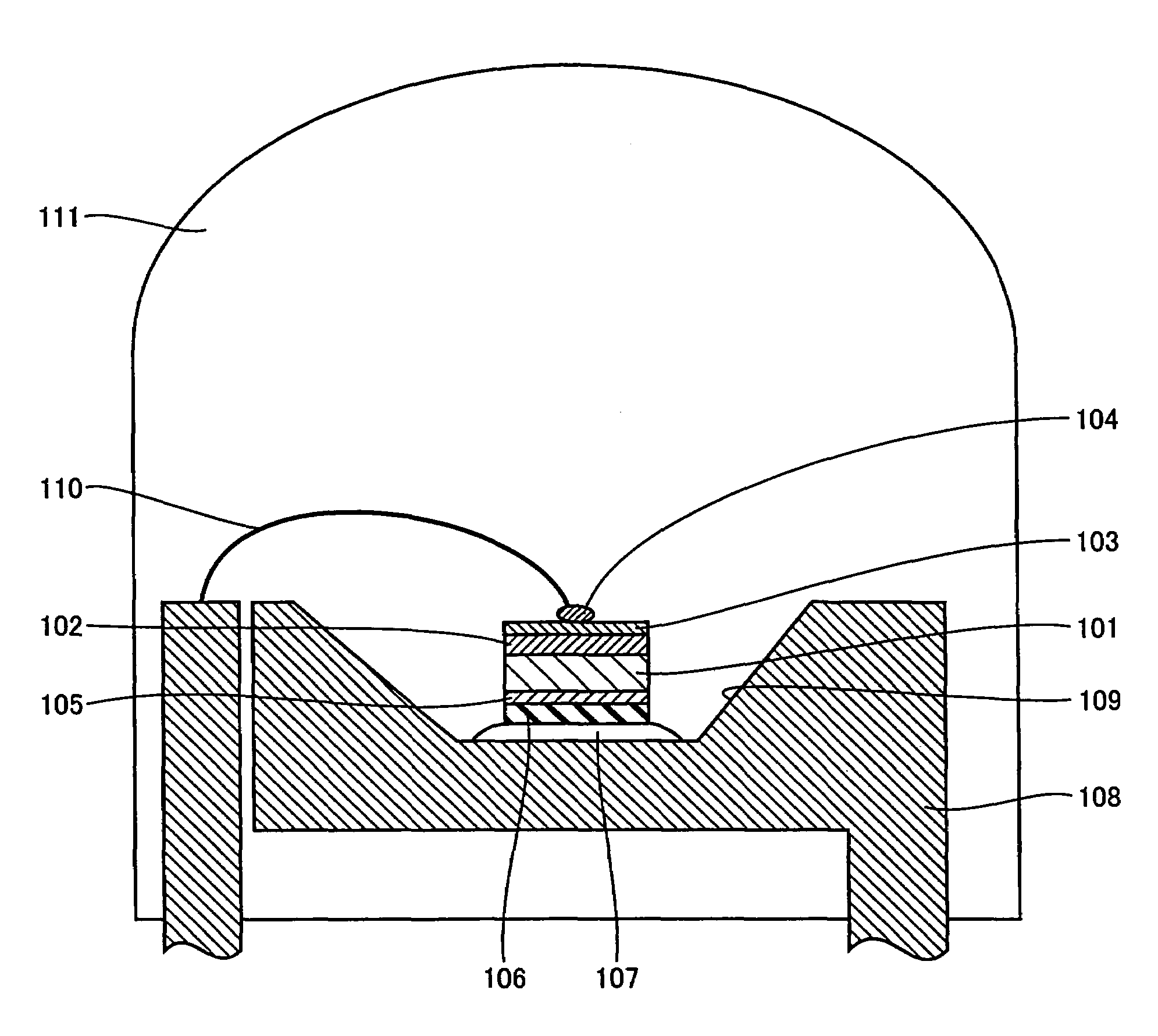
[0021]Referring to FIG. 1, a first embodiment of a semiconductor light-emitting device is described that includes, as a light-emitting element, an LED chip having an n-GaN substrate and a nitride-based compound semiconductor multilayer film formed on the substrate.

[0022]The LED chip includes n-GaN substrate 101 with c-plane (0001) on which nitride-based compound semiconductor multilayer film 102 is formed. Nitride-based compound semiconductor multilayer film 102 includes a buffer layer, an n-GaN cladding layer, a multiple quantum well active layer, a p-AlGaN protective layer, and a p-GaN contact layer that are successively deposited. On the topmost surface of nitride-based compound semiconductor multilayer film 102, a p-type electrode 103 and a P pad electrode 104 are formed. On the rear surface of the substrate, an n-type electrode is formed. The LED chip is 350 μm×350 μm in size.

[0023]The n-type electrode is constituted of a metal layer 105 containing a first metal and a seco...

second embodiment

[0033

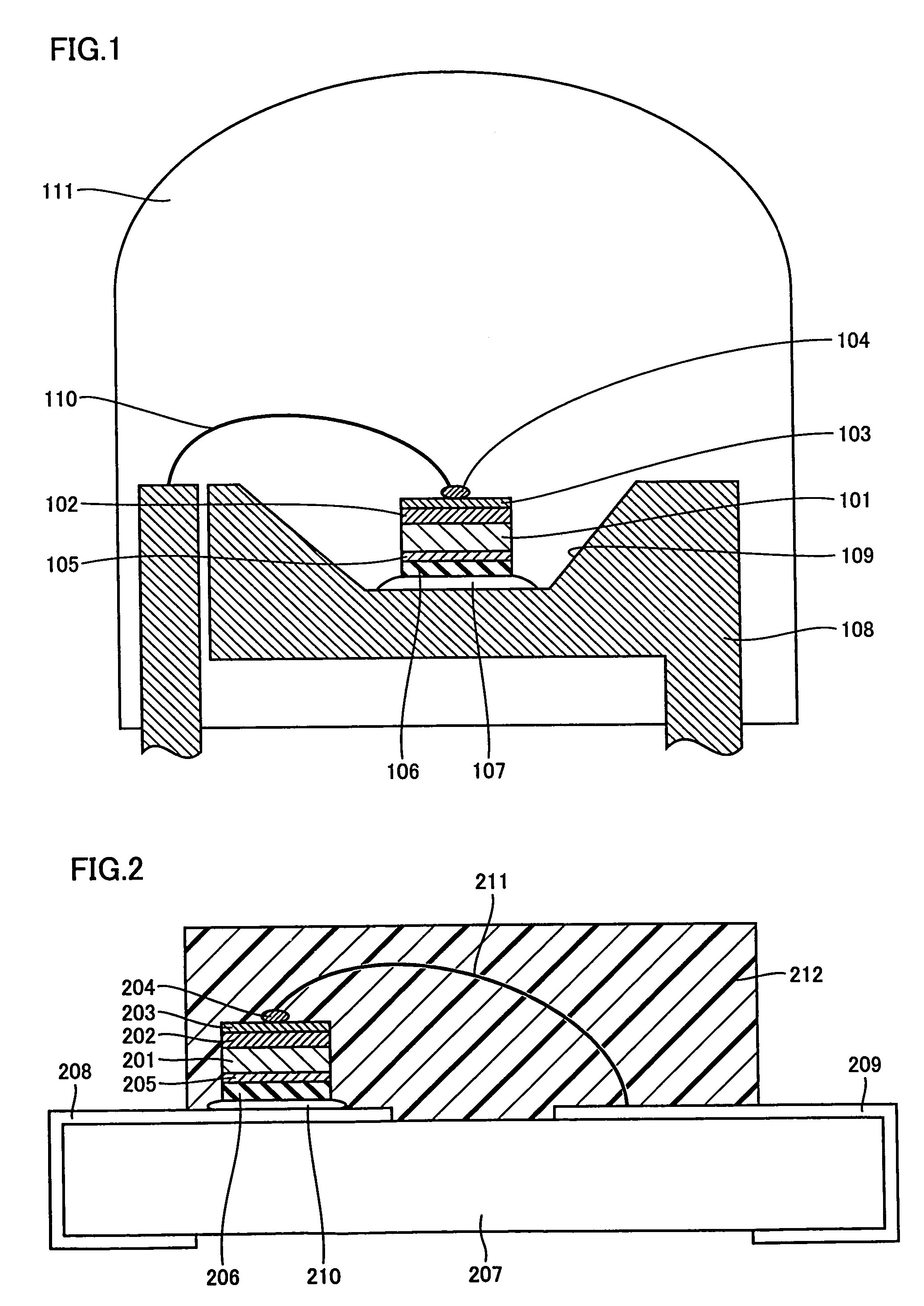
[0034]Referring to FIG. 2, a surface-mount semiconductor light-emitting device is described according to a second embodiment of the present invention. The light-emitting device includes, as a light-emitting element, an LED chip which is directly mounted on a motherboard. Here, the LED chip is the same as that of the first embodiment.

[0035]The surface-mount semiconductor light-emitting device according to the second embodiment includes an LED chip having an n-GaN substrate 201, a nitride-based compound semiconductor light-emitting element 202, a p-type electrode 203, a P pad electrode 204, a metal layer 205, and an ohmic electrode 206. Metal layer 205 contains Hf as a first metal and Al as a second metal.

[0036]On a smooth upper surface of a substrate (motherboard) 207 made of glass epoxy resin, a die bonding electrode pattern 208 and a wire bonding electrode pattern 209 are formed. The LED chip mounted on die bonding electrode pattern 208 is attached to the substrate with Ag pas...

third embodiment

[0038

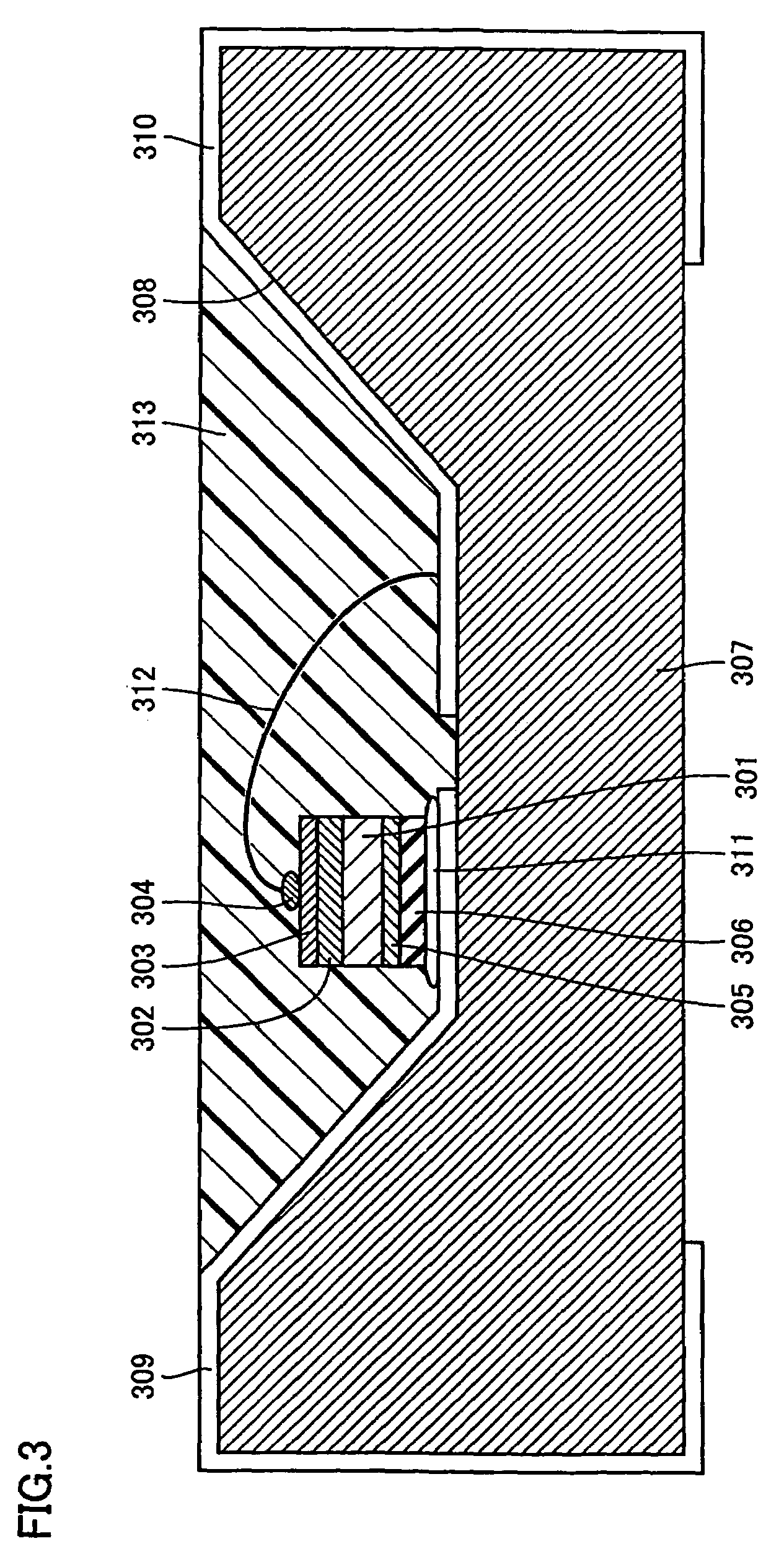
[0039]Referring to the cross sectional view of FIG. 3, a surface-mount semiconductor light-emitting device according to a third embodiment is described. The semiconductor light-emitting device includes an LED chip as a light-emitting element that is directly mounted on a motherboard. Here, the LED chip is the same as that of the first embodiment.

[0040]The surface mount semiconductor light-emitting device according to the third embodiment includes an LED chip having an n-GaN substrate 301, a nitride-based compound semiconductor light-emitting element 302, a p-type electrode 303, a P pad electrode 304, a metal layer 305, and an ohmic electrode 306. Metal layer 305 contains Hf as a first metal and Al as a second metal.

[0041]On the upper side of a block-shaped substrate (motherboard) 307 made of liquid crystal polymer, a recess 308 is formed as a reflective cup. Along the inner wall of recess 308, a die bonding electrode pattern 309 and a wire bonding electrode pattern 310 are form...


PUM

PropertyMeasurementUnit
sizeaaaaaaaaaa
operating voltageaaaaaaaaaa
currentaaaaaaaaaa

Abstract

A nitride-based semiconductor light-emitting device includes a light-emitting element having an n-GaN substrate and a nitride-based semiconductor multilayer film formed on the n-GaN substrate. The n-GaN substrate of the light-emitting element is fixed to a mount surface. The n-GaN substrate has one surface with the nitride-based semiconductor multilayer film formed thereon and an opposite surface with a metal layer and an ohmic electrode formed thereon. The metal layer contains a first metal and a second metal and the ohmic electrode is formed of the second metal. The adhesion between the ohmic electrode and the n-GaN substrate is thus improved. Accordingly, the semiconductor light-emitting device which is highly reliable with respect to the thermal strain from the mount surface can be provided.

Description

BACKGROUND OF THE INVENTION[0001]1. Field of the Invention[0002]The present invention relates to nitride-based semiconductor light-emitting devices.[0003]2. Description of the Background Art[0004]Nitride-based semiconductor is used as a material for high-brightness blue LED (light-emitting diode) and pure green LED that have already been employed for full-color displays for example. Moreover, nitride-based semiconductor is being developed for use in a semiconductor laser as a short-wavelength light source, for the purpose of increasing the storage capacity of an optical disk. These devices have been formed on an insulating sapphire substrate, and thus it is impossible to direct electric current from the rear side of the substrate. Accordingly, p-type and n-type electrodes are formed on the front side, which requires a complicated process for fabricating the electrodes.[0005]According to recently presented reports about fabrication of semiconductor lasers and LEDs, a mask member is p...

Claims


Application Information

Patent Timeline
Patent Type & Authority Patents(United States)
IPC IPC(8): H01L27/15H01L33/00H01L21/28H01L33/32H01L33/40H01L33/56H01L33/62H01S5/02H01S5/0231H01S5/042H01S5/22H01S5/223H01S5/323
CPCH01L33/32H01S5/0425H01S5/32341H01L24/32H01S5/0202H01S5/02244H01S5/2201H01S5/2231H01L2224/48247H01L2224/32257H01L2224/32245H01L2224/48091H01L2924/00014H01L2924/351H01L2924/181H01L2924/12042H01L2924/12041H01S5/04252H01S5/02234H01S5/0231H01S5/02345H01L2924/00
Inventor TATSUMI, MASAKIHATA, TOSHIOFUDETA, MAYUKO
Owner SHARP KK
Why Eureka
Try Eureka