Wafer level stacked package
a stacking and wafer technology, applied in the direction of printed circuit structure associations, semiconductor devices, semiconductor/solid-state device details, etc., can solve the problems of difficult to innovately improve memory capacity or functionality, manufacturing process becomes complex, and it is not possible to stack two or more finished wafer level packages with each other, so as to enhance bonding forces
- Summary
- Abstract
- Description
- Claims
- Application Information
AI Technical Summary
Benefits of technology
Problems solved by technology
Method used
Image

Examples
Embodiment Construction
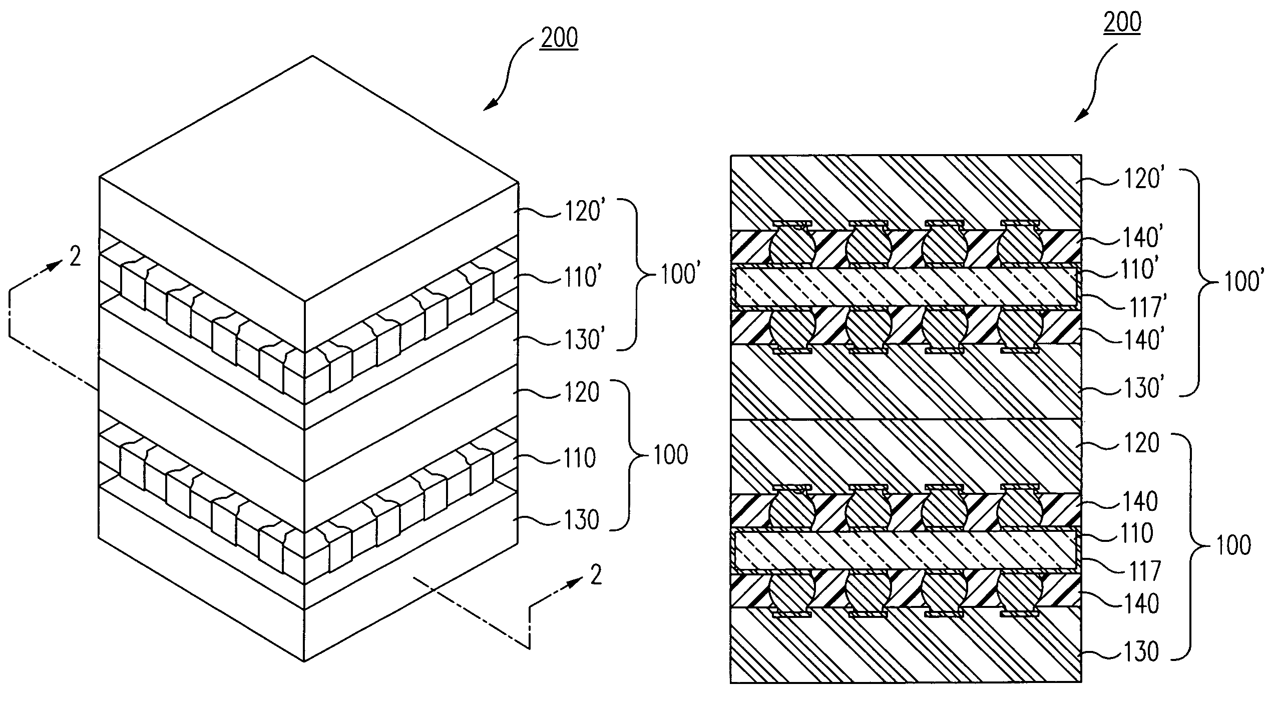
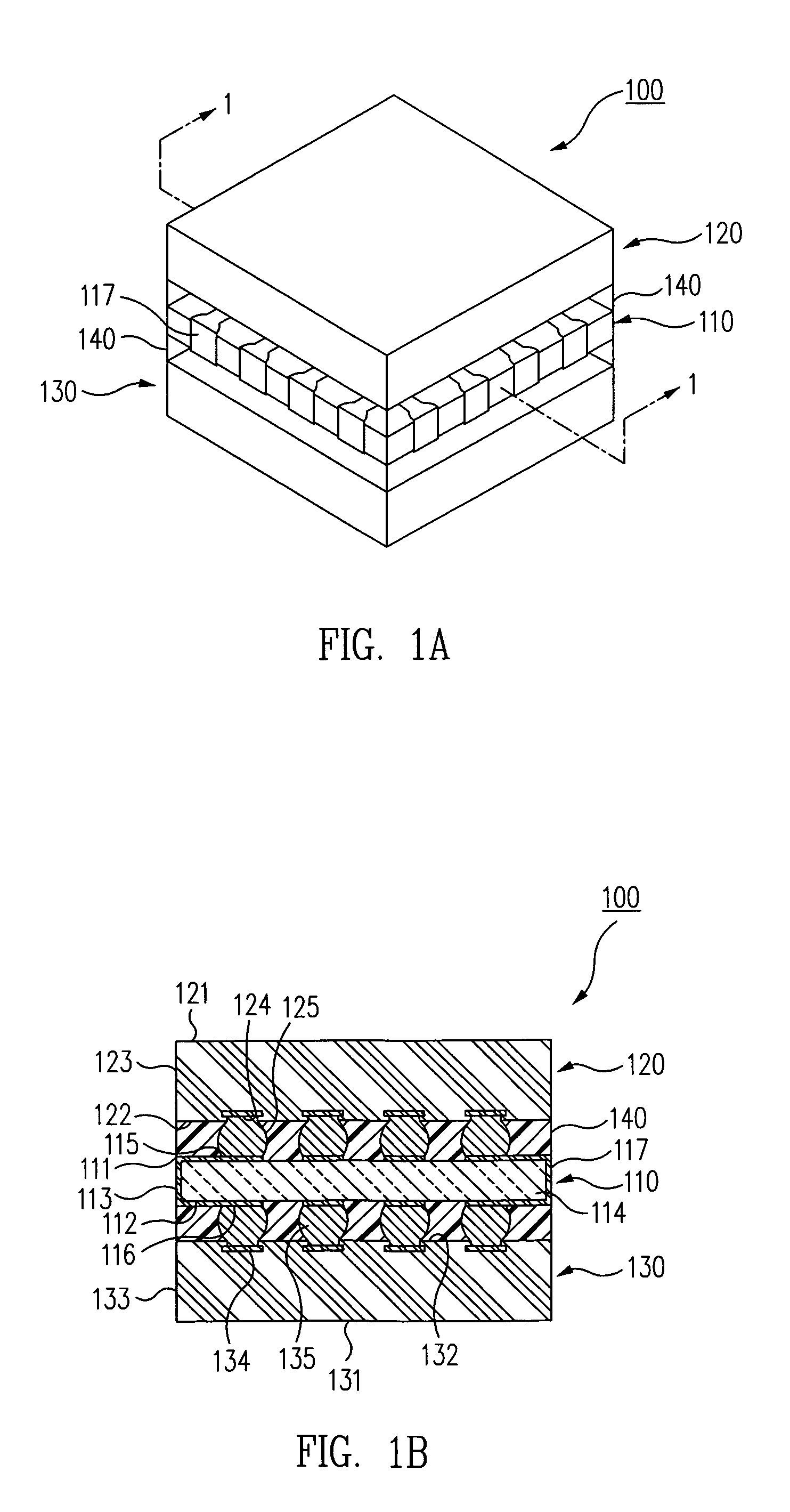
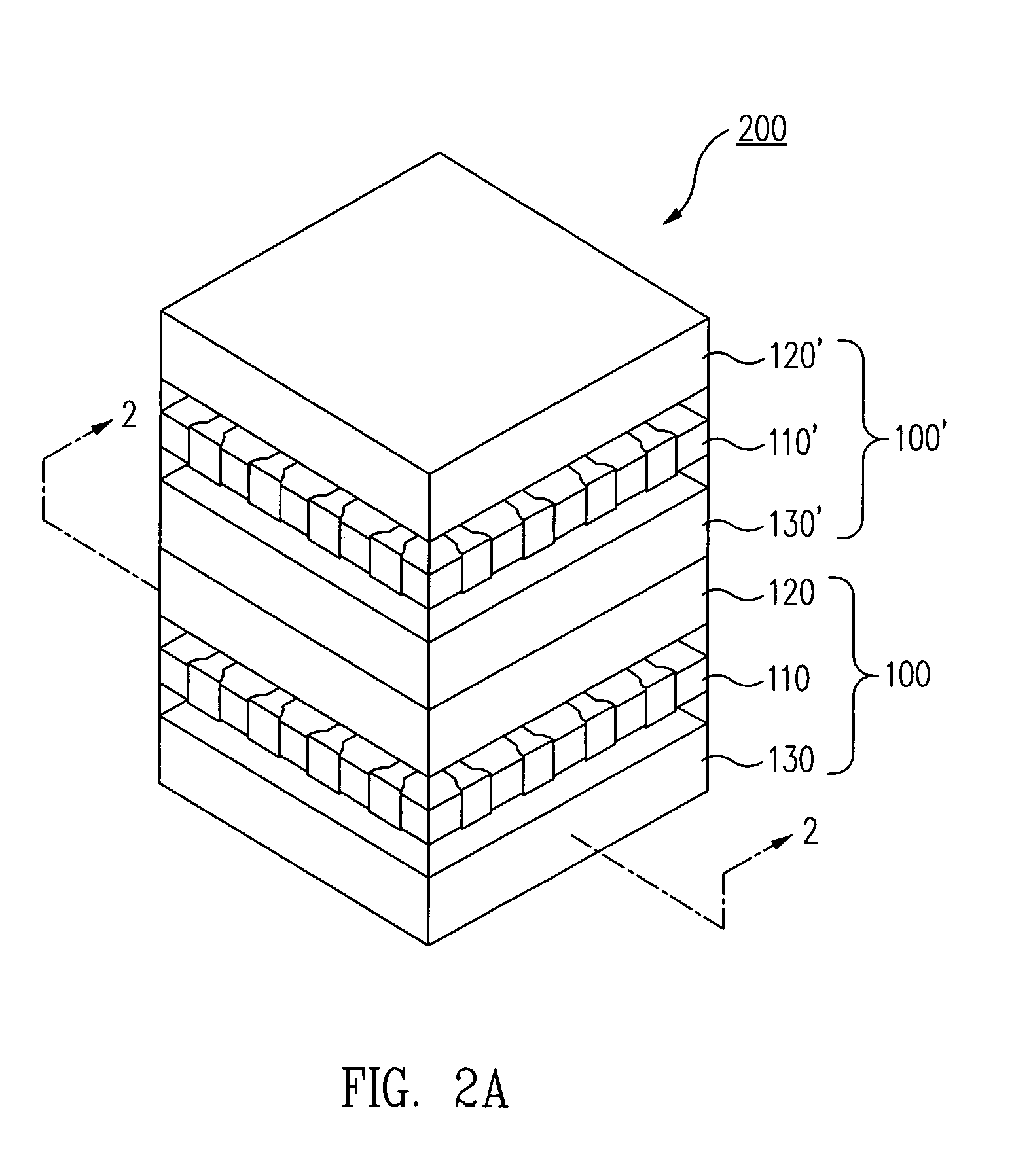
[0024]Referring to FIGS. 1A and 1B, FIG. 1A illustrates a perspective view of a wafer level stacked package in accordance with an embodiment of the present invention and FIG. 1B illustrates a sectional view taken along line 1—1 in FIG. 1A.
[0025]As shown in the drawings, the wafer level stacked package 100 in accordance with this embodiment of the present invention generally includes a substrate 110, a first semiconductor die 120 located on one surface of the substrate 110 and a second semiconductor die 130 located on an opposite surface of the substrate 110.
[0026]First of all, the substrate 110 includes an insulative layer 114 which has a first approximately planar surface 111, a second approximately planar surface 112 opposite to the first surface 111, and four third surfaces 113 formed around and perpendicular to the first and second surfaces 111, 112. Such an insulative layer 114 has a predetermined thickness and may be made of hard material, soft material or equivalents thereof,...
PUM
 Abstract
Description
Claims
Application Information
 - Generate Ideas
- Intellectual Property
- Life Sciences
- Materials
- Tech Scout
- Unparalleled Data Quality
- Higher Quality Content
- 60% Fewer Hallucinations
Browse by: Latest US Patents, China's latest patents, Technical Efficacy Thesaurus, Application Domain, Technology Topic, Popular Technical Reports.
© 2025 PatSnap. All rights reserved.Legal|Privacy policy|Modern Slavery Act Transparency Statement|Sitemap|About US| Contact US: help@patsnap.com