Wafer transfer equipment and semiconductor device manufacturing apparatus using wafer transfer equipment

Inactive Publication Date: 2007-02-06
KK TOSHIBA
View PDF15 Cites 0 Cited by
  • Summary
  • Abstract
  • Description
  • Claims
  • Application Information

AI Technical Summary

Benefits of technology

[0012]According to an embodiment of the present invention, an object of the invention is to obtain a wafer transfer equipment capable of relatively easily alignin

Problems solved by technology

Thus, an accurate adjustment for the pre-positioning was required

Method used


Image

  • Wafer transfer equipment and semiconductor device manufacturing apparatus using wafer transfer equipment
  • Wafer transfer equipment and semiconductor device manufacturing apparatus using wafer transfer equipment
  • Wafer transfer equipment and semiconductor device manufacturing apparatus using wafer transfer equipment

Examples


Example

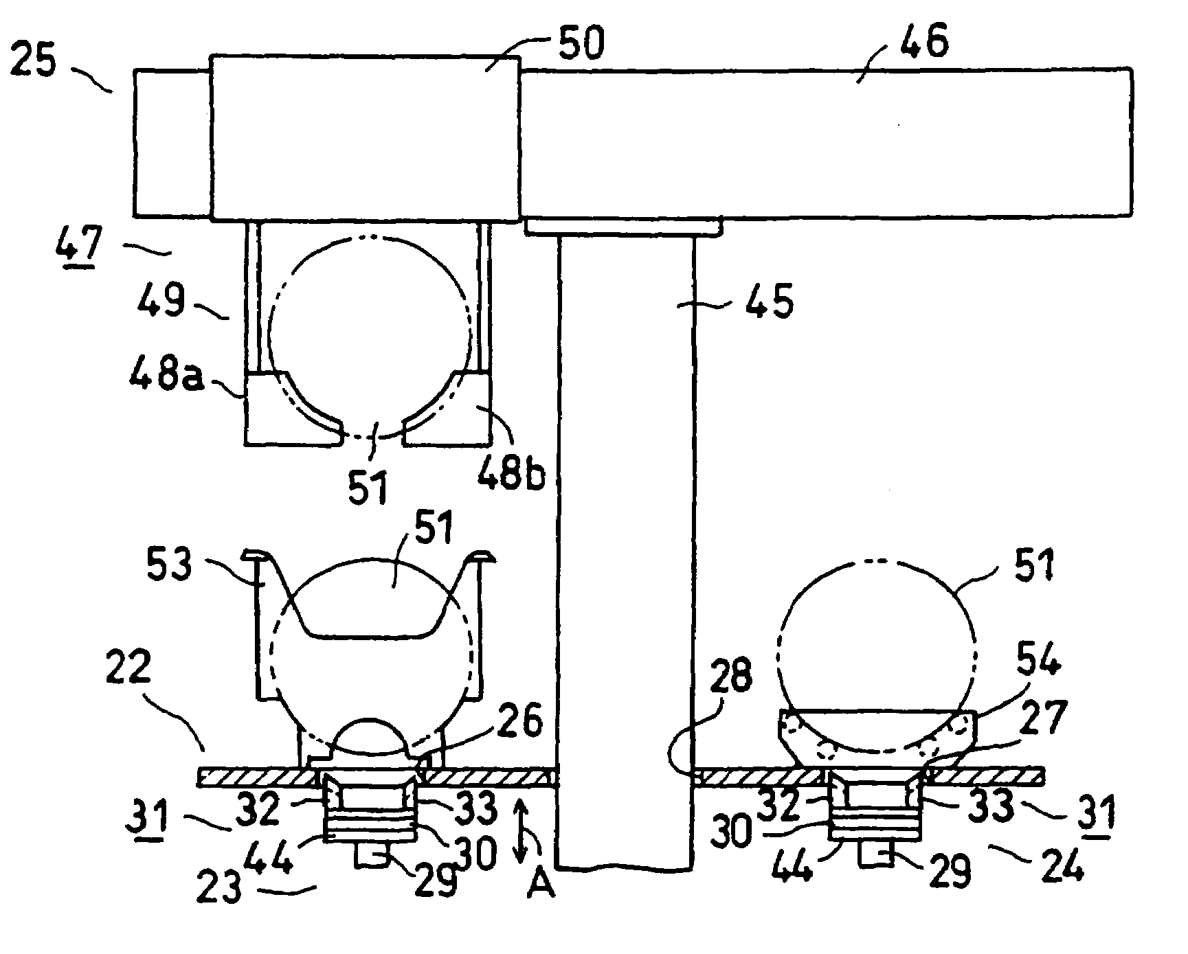
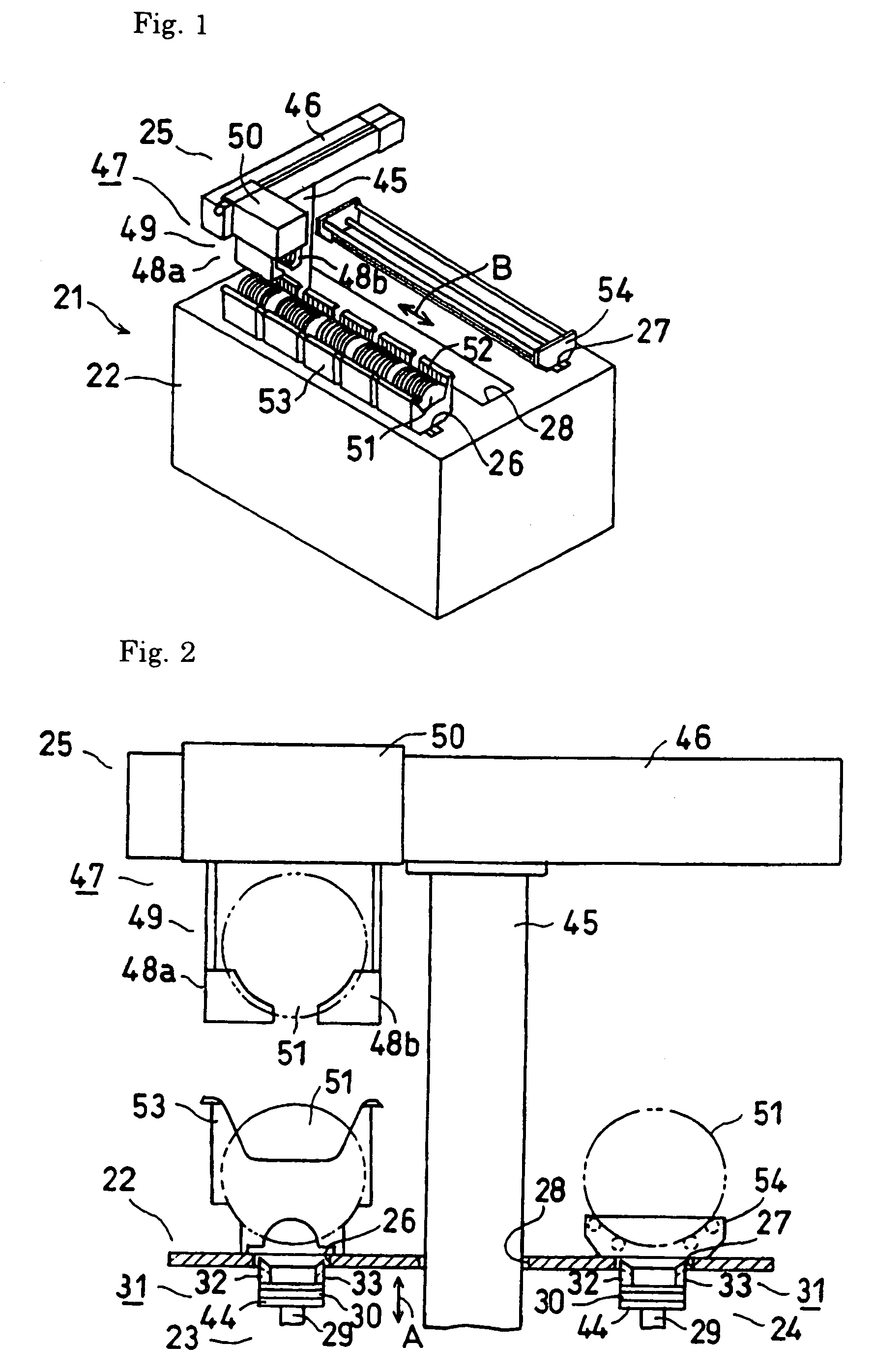
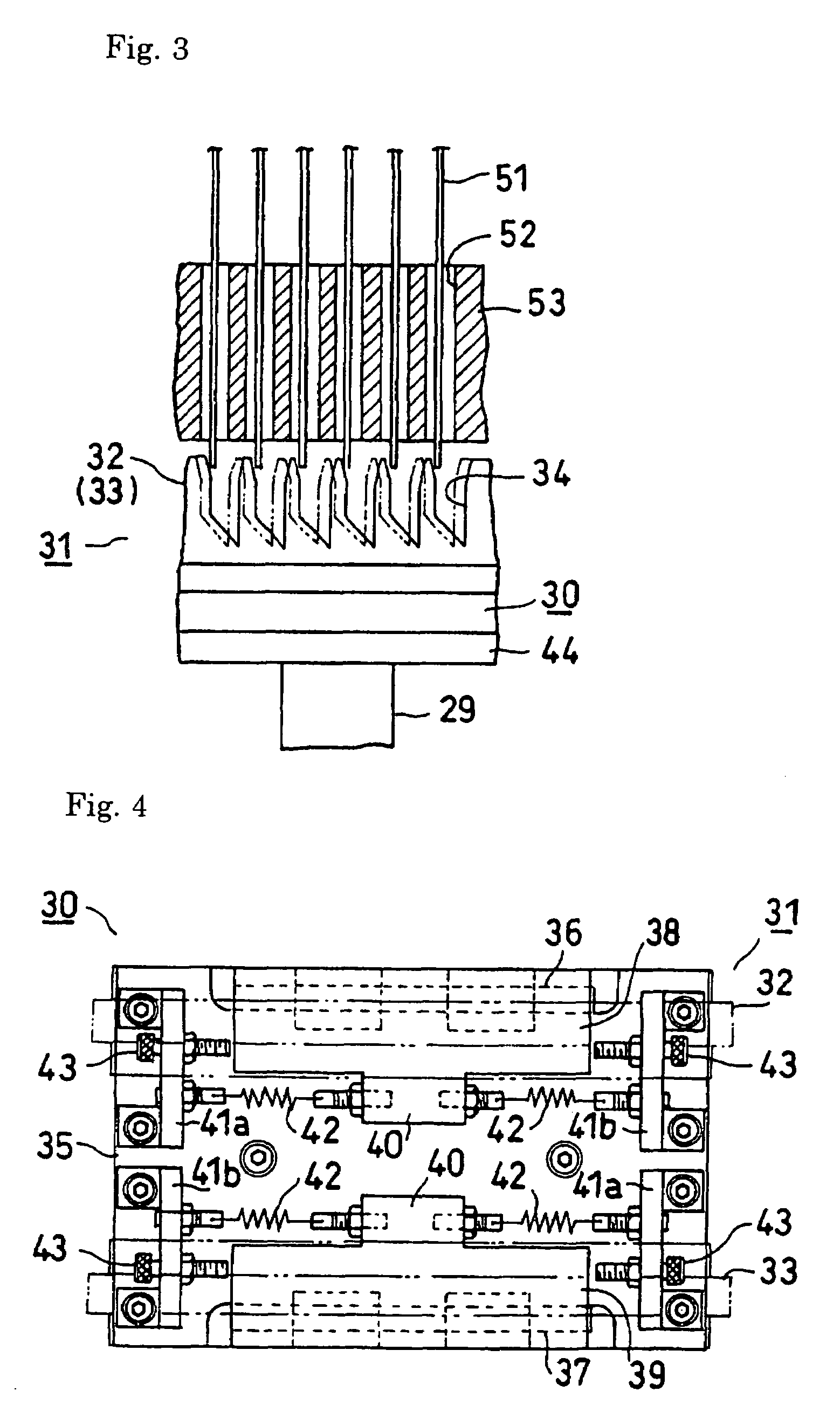
[0036]One embodiment of the present invention will be described below referring to FIG. 1 through FIG. 11. 21 is a semiconductor wafer transfer equipment that is used in such processes as a diffusion process or CVD process. Semiconductor wafer transfer equipment is provided with a first wafer elevator 23 and a second wafer elevator 24, separately on a main body 2. Further, a wafer transfer unit 25 is provided between both wafer elevators 23 and 24. First and second wafer elevators 23 and 24 move through first and second elevating rectangular openings 26 and 27 on the top of main body 22 up and down as shown by an arrow A with a drive unit (not illustrated) provided in main body 22 from the inner specified position to an external position at a specified height. Further, first and second wafer elevators 23 and 24 move back and forth in the longitudinal opening direction that is the cross direction of main body 22, as shown by the arrow B.

[0037]Wafer transfer unit 25 is also moved back...


PUM


Abstract

A semiconductor wafer transfer equipment transfers a plurality of semiconductor wafers, held in grooves of carriers in an erected state, to a boat using first and second wafer elevators equipped with a comb-teeth portion and a wafer grip and transfer unit. The first and second wafer elevators correspond to the carriers and the boat and are equipped with a position correction mechanism which corrects positions of comb-teeth openings of comb-teeth members provided on the comb-teeth portion, corresponding to semiconductor wafers housed in the grooves of the carriers.

Description

CROSS-REFERENCE TO RELATED APPLICATIONS[0001]This application is based upon and claims the benefit of priority from the prior Japanese Patent Application No. 2003-178389, filed on 23rd June, 2003; the entire contents of which are incorporated herein by reference.BACKGROUND OF THE INVENTION[0002](1) Field of the Invention[0003]The present invention relates to a wafer transfer equipment that is used when, for example, semiconductor wafers are transferred to a batch processing between wafer carriers and boats and a semiconductor device manufacturing apparatus using this wafer device transfer equipment.[0004](2) Description of the Related Art[0005]A conventional technology will be described below referring to FIG. 12 and FIG. 13. A semiconductor wafer transfer equipment is provided with a first wafer elevator 3 that moves up and down from an internal specific position in a main body 2 of the equipment 1 to an external position at a specific height and a second wafer elevator 4 that move...

Claims


Application Information

Patent Timeline
IPC IPC(8): B65G65/00B65G49/07H01L21/677H01L21/68
CPCH01L21/67781
Inventor FUJII, KOJITAKEUCHI, TOMOAKI
Owner KK TOSHIBA
Why Eureka
Try Eureka