

Network conductor and its production method and use
a network conductor and conductor technology, applied in the field of network conductors, can solve the problems of poor energy efficiency and driving durability, uneven brightness, and the need for a higher driving voltage of organic el devices, and achieve the effects of low resistivity, high light transmittance, and excellent charge injection properties
- Summary
- Abstract
- Description
- Claims
- Application Information
AI Technical Summary
Benefits of technology
Problems solved by technology
Method used
Image

Examples
example 1
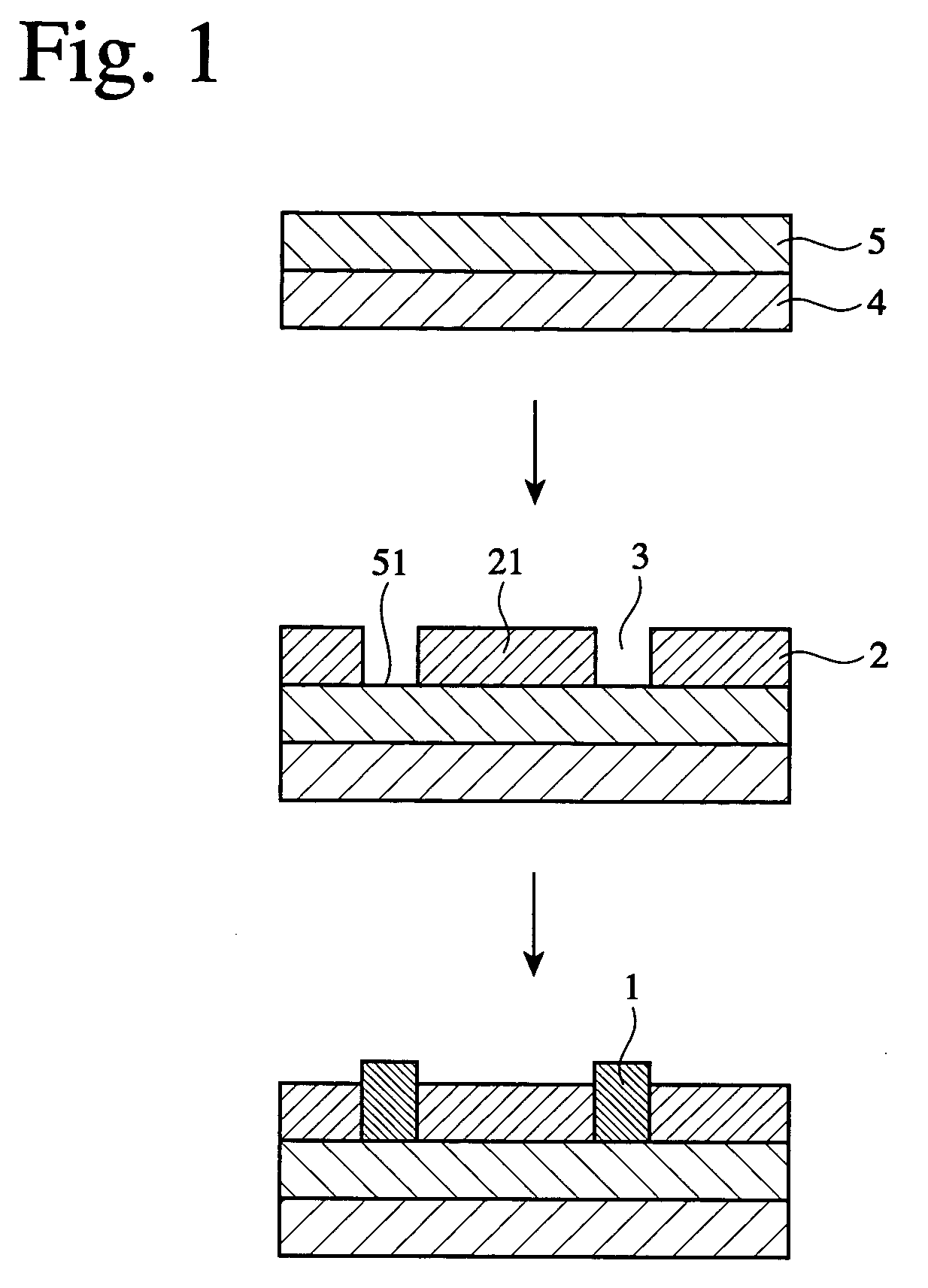
Production of Network Conductor-having Substrate
(1) Preparation of Plated Underlayer
[0144]Palladium chloride was reduced by sodium borohydride in a dispersion solvent of heptane / water to obtain a dispersion liquid of Pd metal particles having the average particle size of 5 nm. 5% by mass of polymethyl methacrylate was added to the dispersion liquid based on 100% by mass of the Pd metal particles, and diluted with toluene to prepare a coating liquid. A 50 μm (thickness)×25 mm×25 mm in size of a substrate made of ZEONOR 1020R available from Zeon Corporation was subjected to a corona discharge treatment, and the coating liquid was applied by a spin coater to the substrate, to form a plated underlayer. Then, the plated underlayer was subjected to an alkali edging treatment using 2N aqueous sodium hydroxide solution at 70° C. for 1 hour.
(2) Preparation of Sol-gel Film
[0145]Water, hydrochloric acid, and propyl alcohol were added to tetraethoxysilicate and stirred at ambient temperature fo...
example 2
Production of Organic EL Device
[0147]A transparent conductive layer of indium tin oxide (ITO, indium / tin=95 / 5 by mol) was formed into the 0.2 μm thickness by a sputtering method using a direct-current power source on the sol-gel film containing the network conductor of the network conductor-having substrate obtained in Example 1. Thus, a positive electrode comprising the network conductor layer of silver and the transparent conductive layer of ITO was obtained. The positive electrode had the surface resistance of 4 Ω / square. A dichloroethane solution of a composition of polyvinyl carbazole / 1,1,4,4-tetraphenylbutadiene (blue light-emitting material) / tris(2-phenylpyridine) iridium complex (green light-emitting material of ortho-metallation complex) / 4-(dicyanomethylene)-2-methyl-6-(4-dimethylaminostyryl)-4H-pyran (red light-emitting material) / 2-(4-biphenylyl)-5-(4-t-butylphenyl)-1,3,4-oxadiazole (electron-transporting material)=200 / 1 / 5 / 1 / 50 (weight ratio) was applied by a spin coater o...
example 3
Production of Network Conductor-having Substrate
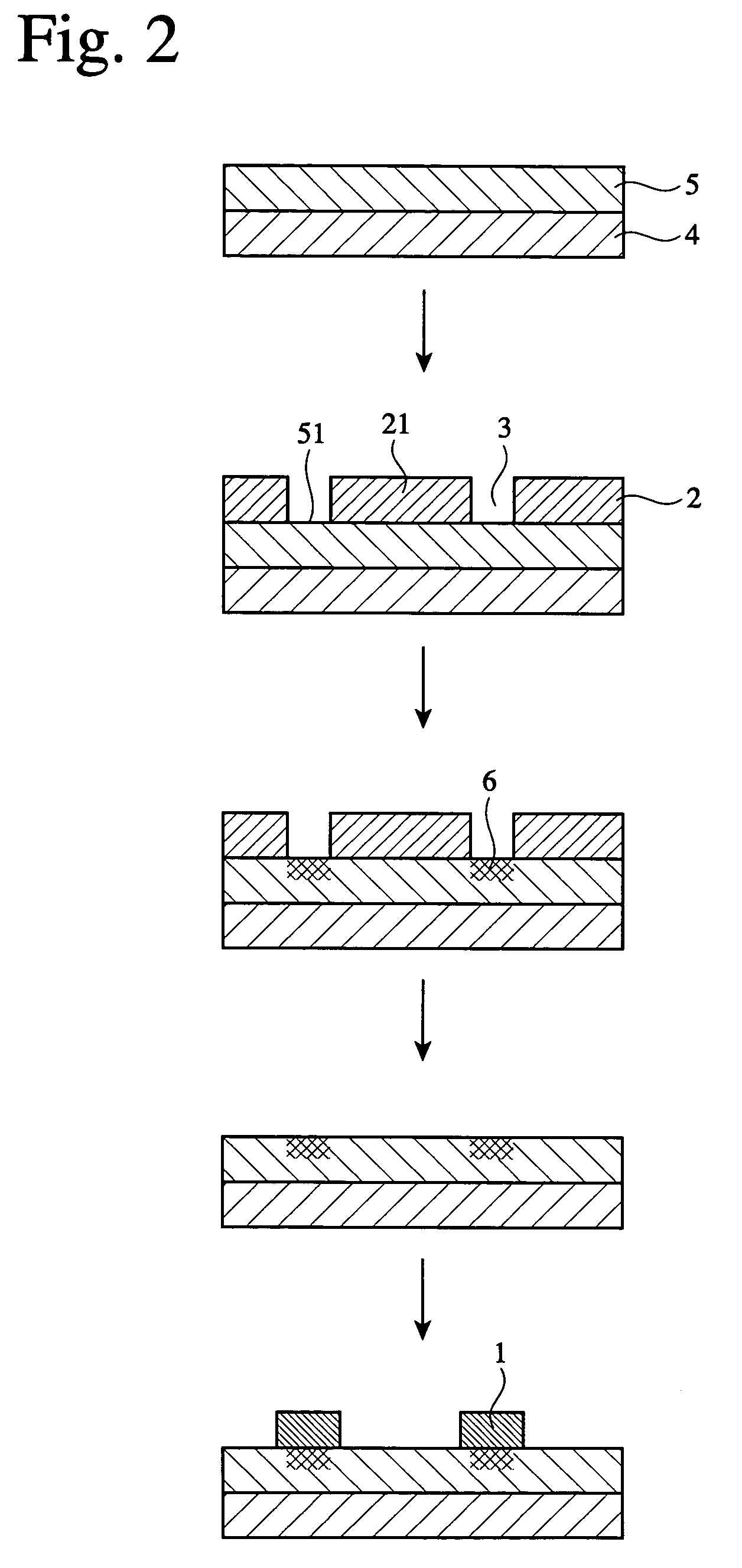
(1) Preparation of Bondable Underlayer
[0151]1 g of 3-mercaptopropyltrimethoxysilane was added to 100 ml of an aqueous solution containing 1% by mass of acetic acid, and stirred to make the resultant mixture uniform. The obtained sol liquid was applied by a spin coater onto a glass substrate having a size of 0.7 mm in thickness×25 mm×25 mm, and heated at 120° C. for 1 hour, to form a bondable underlayer.
(2) Preparation of Sol-gel Film
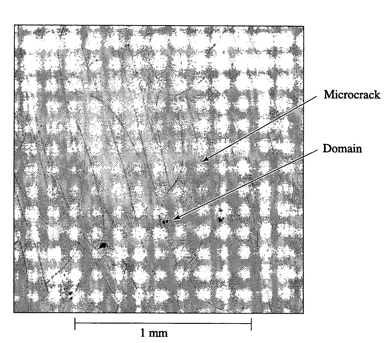
[0152]A sol-gel film was formed on the bondable underlayer obtained in (1) in the same manner as in Example 1. The sol-gel film had the thickness of 0.4 μm after drying. As a result of observing the sol-gel film by an optical microscope, the sol-gel film was cracked, and microcracks and domains surrounded by the microcracks were found.
(3) Preparation of Conductive Particles
[0153]An aqueous sodium citrate solution as a reducing agent was added to an aqueous chloroauric (III) acid solution, and the mixture wa...
PUM
| Property | Measurement | Unit |
|---|---|---|
| work function | aaaaa | aaaaa |
| work function | aaaaa | aaaaa |
| resistivity | aaaaa | aaaaa |
Abstract
Description
Claims
Application Information