Optical-interference type display panel and method for making the same

a display panel and optical interference technology, applied in the manufacture of electric discharge tubes/lamps, identification means, instruments, etc., can solve the problems of metal wires becoming gradually oxidized, back light modules consuming the most power of all elements, and affecting so as to improve the reliability of connecting pads, the effect of excellent anti-oxidation ability and excellent anti-oxidation ability

Inactive Publication Date: 2007-02-06
SNAPTRACK
View PDF400 Cites 149 Cited by
  • Summary
  • Abstract
  • Description
  • Claims
  • Application Information

AI Technical Summary

Benefits of technology

[0016]Since said connecting pads are made of a transparent conductive layer composed in said first optical conductive optical film stacks, these connecting pads have the excellent anti-oxidation ability at their surface. Thus, the connecting quality and the reliability of the connecting pads are improved.

Problems solved by technology

Inside the LCD device, the back light module consumes the most power of all the elements.
Even though these thin films are pervious to light, a partial amount of light may be blocked or lost while light passes through these films.
However, because the connecting pads are exposed to the air, these metal wires may become gradually oxidized.
Thus, the connecting quality and reliability of the connecting pads may be impaired by the oxidization problem.

Method used


Image

  • Optical-interference type display panel and method for making the same
  • Optical-interference type display panel and method for making the same
  • Optical-interference type display panel and method for making the same

Examples


Embodiment Construction

[0030]With reference to FIGS. 1A to 1E, a basic manufacturing process of an optical interference panel in accordance with the present invention is disclosed. The process includes the following steps.

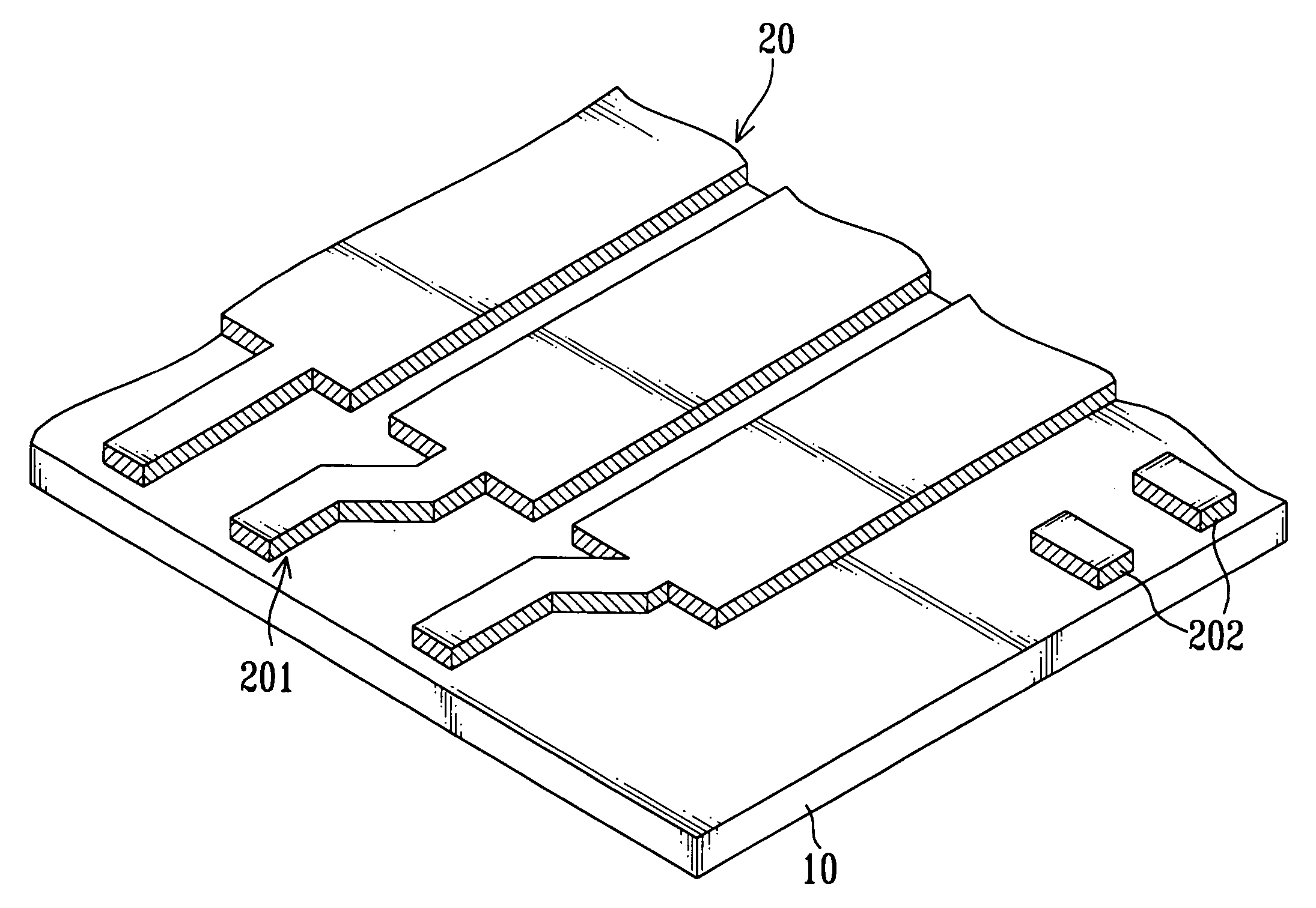
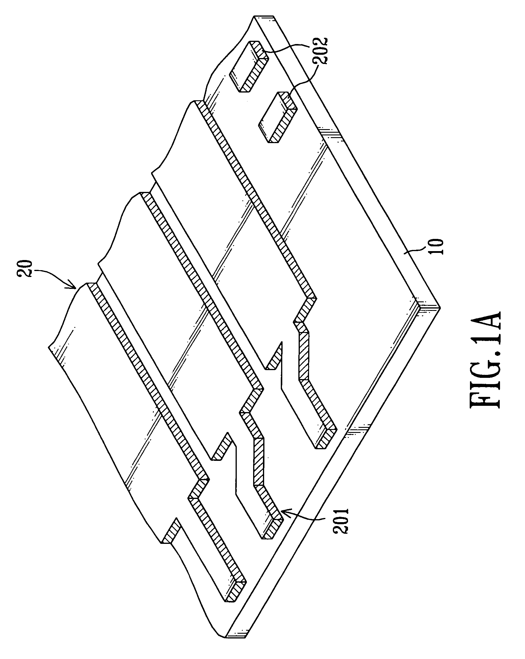
[0031]Forming a plurality of separated first conductive optical film stacks (20) on a substrate (10): these separated first conductive optical film stacks (20) are formed on the substrate (10) that is composed of glass or macromolecule material.

[0032]Defining patterns of connecting pads: portions of these first conductive optical film stacks (20) are further patterned to form multiple connecting pads (201)(202) near the edge of the substrate (10) (as shown in FIG. 1A).

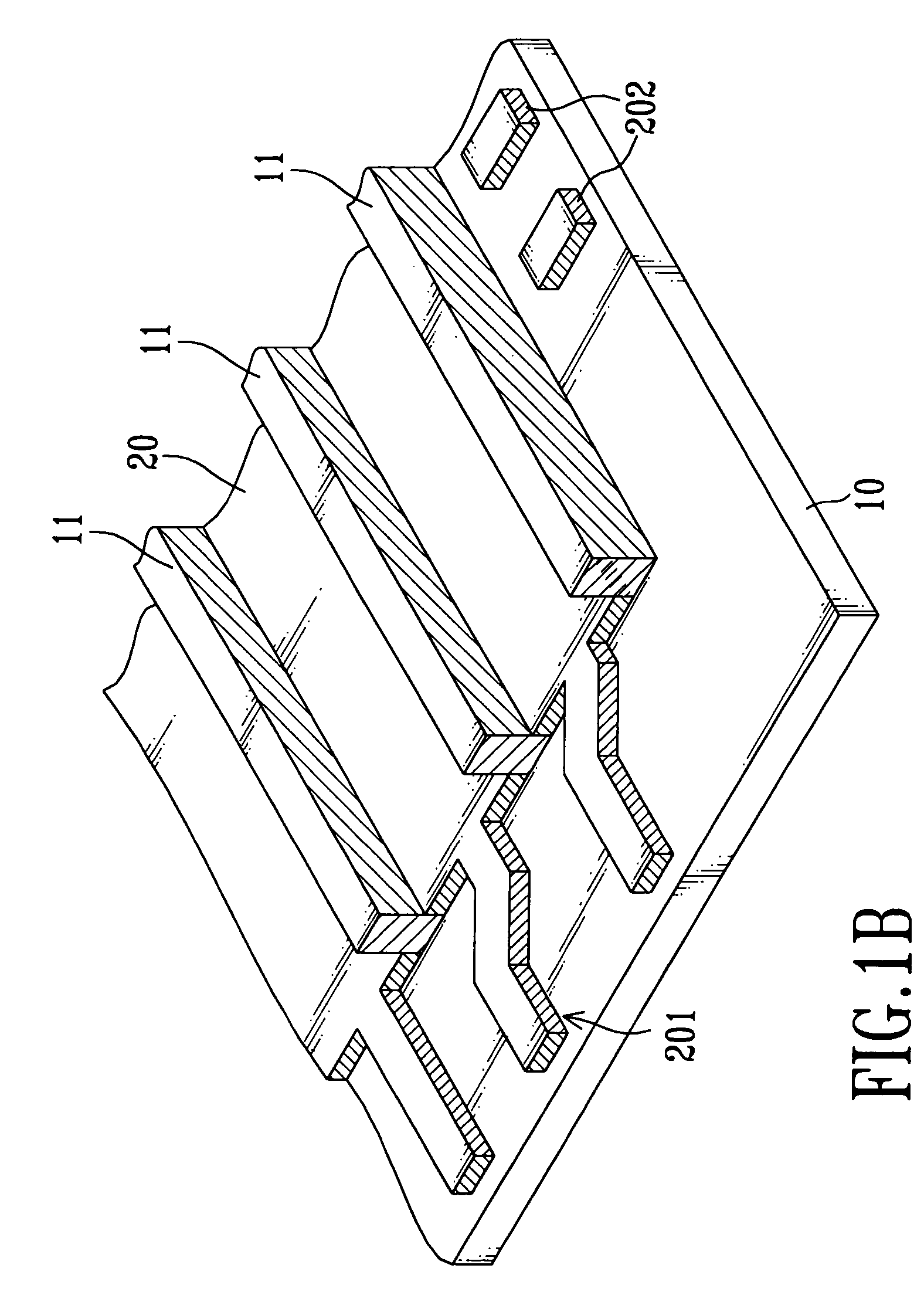
[0033]Forming a supporting layer (11) on the substrate (10): a supporting layer (11) is formed on the substrate (10) where the first conductive optical film stack (20) is removed. That is, the supporting layer (11) is formed between two separated first conductive optical film stacks (20) (as shown in FIG. 1B).

[0034]Forming ...


PUM

PropertyMeasurementUnit
conductiveaaaaaaaaaa
transparentaaaaaaaaaa
sizeaaaaaaaaaa

Abstract

An optical-interference type display panel and a method for making the same are disclosed, wherein the display panel has a substrate on which multiple first conductive optical film stacks, supporting layers and multiple second conductive optical film stacks are formed. The substrate further has a plurality of connecting pads consisting of a transparent conductive film of the first conductive optical film stacks. Since the transparent conductive film is made of indium tin oxide, these connecting pads have the excellent anti-oxidation ability at their surface.

Description

BACKGROUND OF THE INVENTION[0001]1. Field of the Invention[0002]The present invention relates to an optical-interference type display panel and a method for making the same, and more particularly to a display panel in which a transparent conductive layer is employed to form connecting pads for connection to a driving circuit of the panel.[0003]2. Description of Related Art[0004]In order to minimize the bulky size of a computer display, the flat display was developed to replace the conventional CRT display. For example, the most well known flat display is the LCD. In recent years, different kinds of LCDs have been developed by display manufacturers. Most of these manufacturers are dedicated as far as possible to reduce the power consumption of the display so that the LCD will become more suitable for portable electronic products such as cell phones, PDAs and E-books.[0005]Inside the LCD device, the back light module consumes the most power of all the elements. To solve the problem, a...

Claims


Application Information

Patent Timeline
Patent Type & Authority Patents(United States)
IPC IPC(8): H01L21/00G02B26/00H01J9/00G02F1/1335G09F9/00G09F9/30
CPCG02B26/001G02F1/1335
Inventor LIN, WEN-JIANHSU, HUNG-HUEITSAI, HSIUNG-KUANG
Owner SNAPTRACK
Why Eureka
Try Eureka