Layout verification method and method for designing semiconductor integrated circuit device using the same

a technology of integrated circuit devices and verification methods, applied in individual semiconductor device testing, semiconductor/solid-state device testing/measurement, instruments, etc., can solve problems such as severe problems, deterioration of hot carrier life, and broken gate oxide films, and achieve design more efficiently, high accuracy, and high quality.

Inactive Publication Date: 2007-02-06
SOCIONEXT INC
View PDF6 Cites 18 Cited by
  • Summary
  • Abstract
  • Description
  • Claims
  • Application Information

AI Technical Summary

Benefits of technology

[0017]The present invention was developed in consideration of the aforementioned situation. It is an object of the invention to provide a layout verification method capable of accurately detecting damage to be given to a gate.
[0018]It is another object of the invention to provide a higher-workability and higher-reliability design method to accurately detecting damage to be given to a gate and to determine an approach for design correction to avoid plasma charging damage.

Problems solved by technology

This current leads to such problems that the gate oxide film may be broken, the transistor characteristics may change due to a change in film quality of the gate oxide film, or the hot carrier life may deteriorate.
Such antenna damage leads to a severer problem with advance of finer process technologies.
However, in current design rules, it is the that antenna rules tend to deteriorate.
Secondly, the minimum gate width is reduced with finer process technology, but the wiring length cannot be made so short in spite of the finer process technology.
Thirdly, at the time of over-etching in a dry etching step of wiring, damage caused by plasma invading from a side wall of the wiring is a principal factor of the antenna damage.
In order to secure resistance to electro-migration in the wiring or suppress the resistance value, however, there is a tendency that the wiring width can be reduced but the wiring film thickness cannot be made so thin.
Due to the factors described above, an antenna ratio of about several thousands in recent fine process technologies leads to occurrence of antenna damage such as breakdown of a gate oxide film or characteristic deterioration of a transistor in the middle of a manufacturing process of an LSI designed quite commonly although an antenna ratio of about 100 thousand has not leaded to any problem in a conventional CMOS generation based on 0.8 design rules or the like.
However, due to thinner thickness of gates of transistors as a result of recent finer design technologies, there has been observed a phenomenon that the effect of a diode as a protection circuit cannot be obtained sufficiently, or a phenomenon of charging up to a gate terminal from wiring connected to a source or a drain of a transistor.
Thus, huge time and quantity of work are required, but the design quality also deteriorates due to excessive measures or correction.
In addition, in the background-art plasma charging damage verification, there is a problem that the verification step is so complicated that the workability deteriorates when the verification is to be performed accurately.

Method used


Image

  • Layout verification method and method for designing semiconductor integrated circuit device using the same
  • Layout verification method and method for designing semiconductor integrated circuit device using the same
  • Layout verification method and method for designing semiconductor integrated circuit device using the same

Examples


Embodiment Construction

[0079]An embodiment of the invention will be described below. Not to say, the invention is not limited to the embodiment which will be described below.

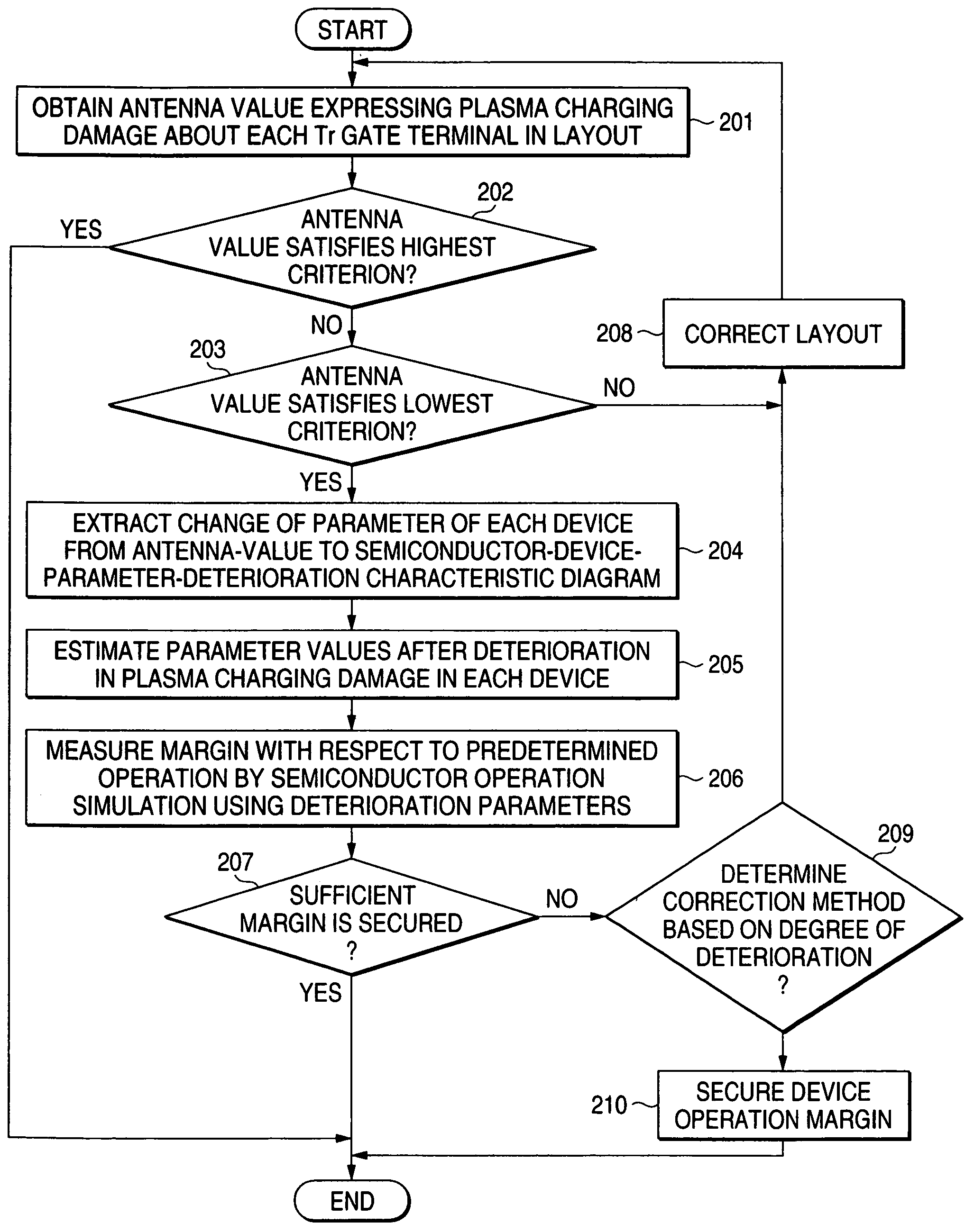
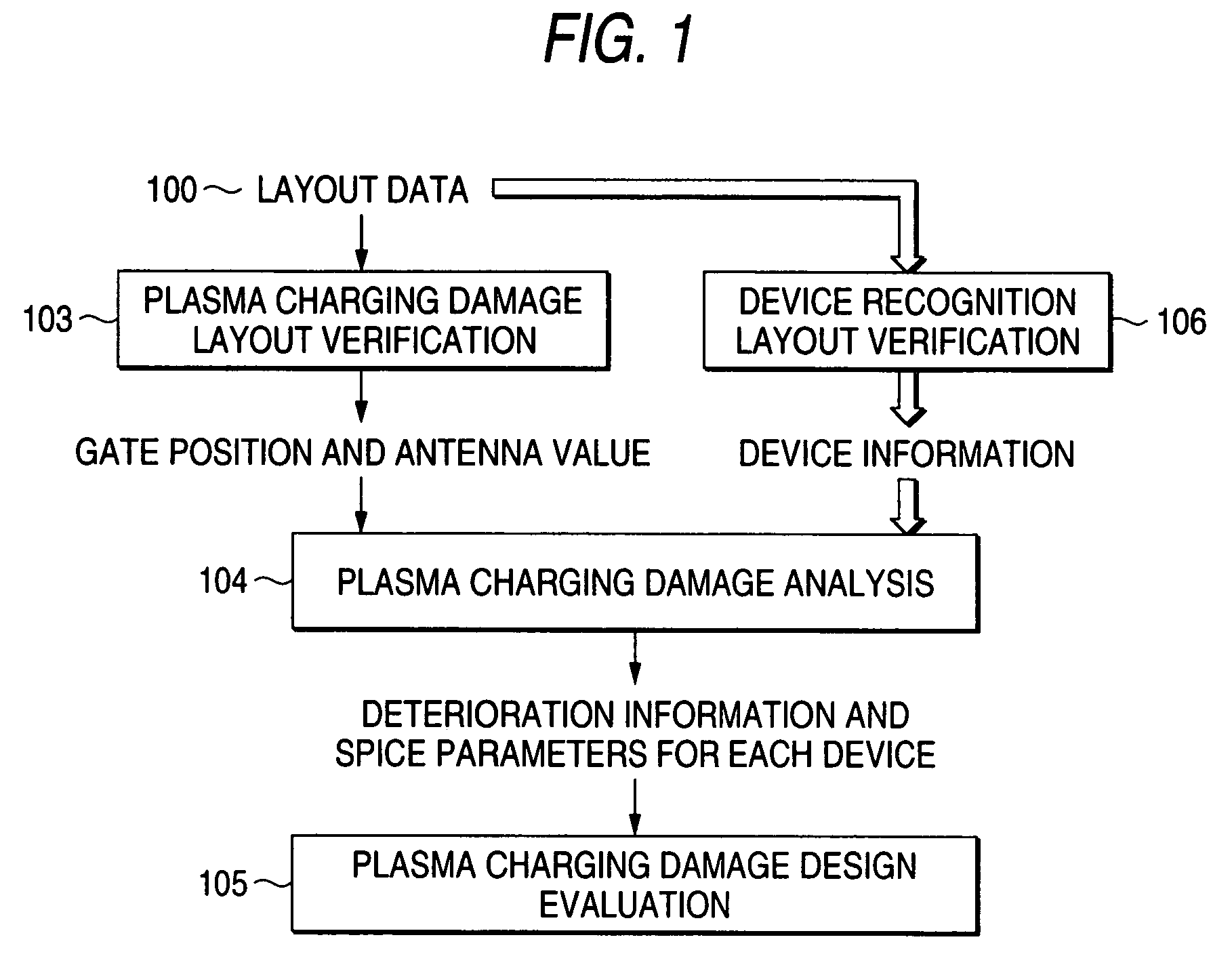
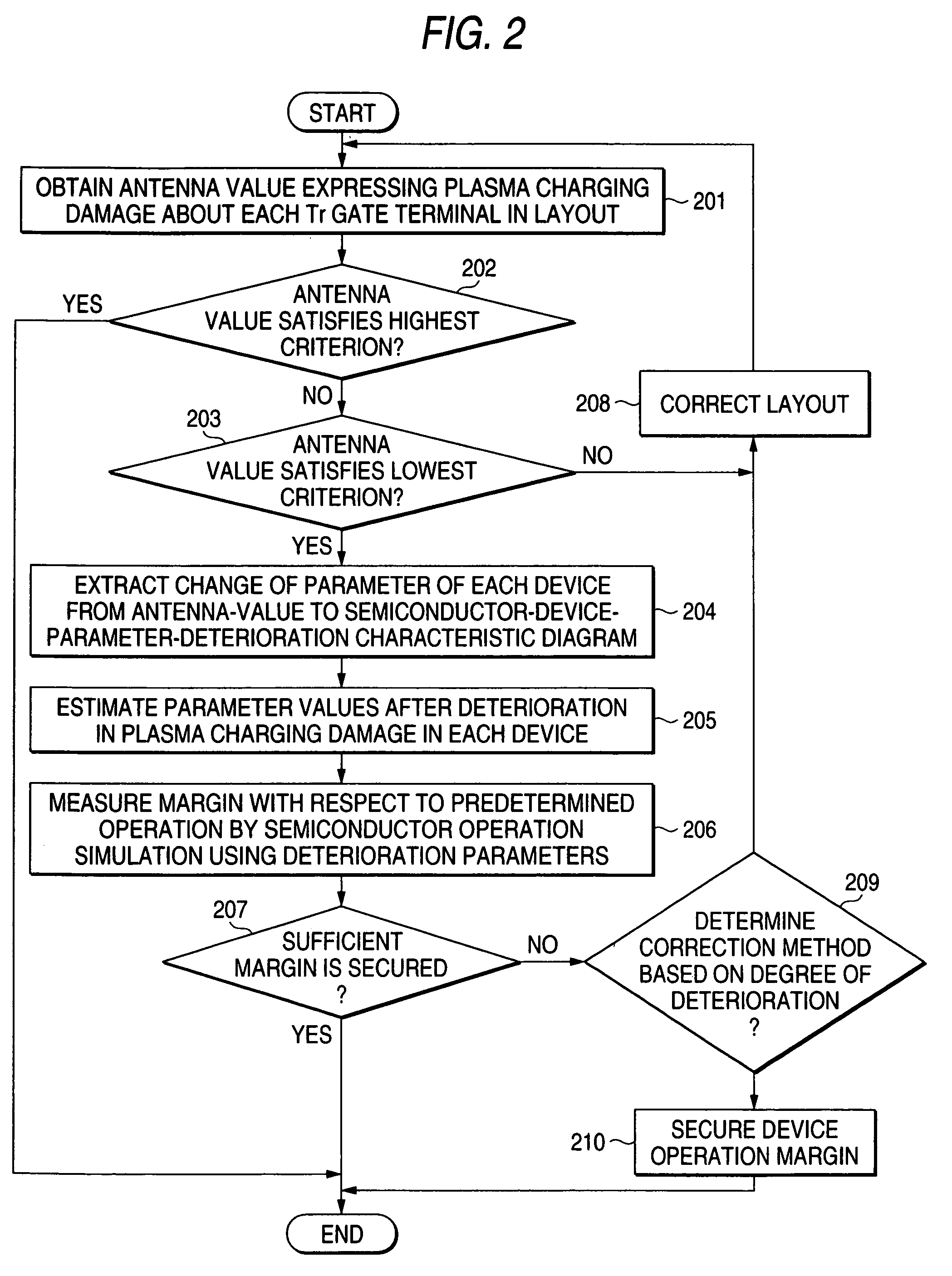
[0080]FIG. 1 shows a schematic block diagram showing a method for analyzing plasma charging damage according to the invention. FIG. 2 shows a flow charge of analysis using this analysis method.

[0081]As shown in FIG. 1, a plasma charging verification step 103 according to the embodiment is characterized in that an antenna value expressing the magnitude of the plasma charging damage is obtained with higher accuracy based on an antenna ratio which is a ratio of an area of a conductor connected to a transistor gate and suffering plasma to an area of the gate, and a fluctuation of the plasma charging damage due to a layout state including the layout near the transistor gate, and layout verification is executed based on the obtained antenna value. The plasma charging verification step 103 is characterized by including an input unit for inpu...


PUM


Abstract

To provide a layout verification method capable of accurately detecting damage to be given to a gate, and to provide a higher-workability and higher-reliability design method to accurately detect damage to be given to a gate and to determine an approach for design correction to avoid damage, the layout verification method according to the invention is characterized in that an antenna value which is an estimated value of transistor gate damage is output based on an antenna ratio, and a fluctuation of plasma charging damage due to the layout near the transistor gate.

Description

BACKGROUND OF THE INVENTION[0001]1. Field of the Invention[0002]The present invention relates to a layout verification method and a method for designing a semiconductor integrated circuit device using the same, and particularly relates to a method for more properly and more accurately verifying plasma charging damage caused by an antenna effect at the time of manufacturing a semiconductor, making proper correction and designing a proper new semiconductor integrated circuit device.[0003]2. Description of the Related Art[0004]In recent years, in processes for manufacturing semiconductor integrated circuit devices, various plasma techniques have been used as methods for enhancing reactivity due to use of plasma so as to implement an active process while reducing the processing temperature. For example, representative ones of the techniques include dry etching at the time of patterning a wiring layer, deposition of a plasma TEOS film for forming an interlayer insulating film to be dispo...

Claims


Application Information

Patent Timeline
Patent Type & Authority Patents(United States)
IPC IPC(8): G06F17/50
CPCH01L22/14H01L2924/0002H01L2924/00
Inventor ITOU, MASANORIMUKAI, KIYOHITO
Owner SOCIONEXT INC
Why Eureka
Try Eureka