

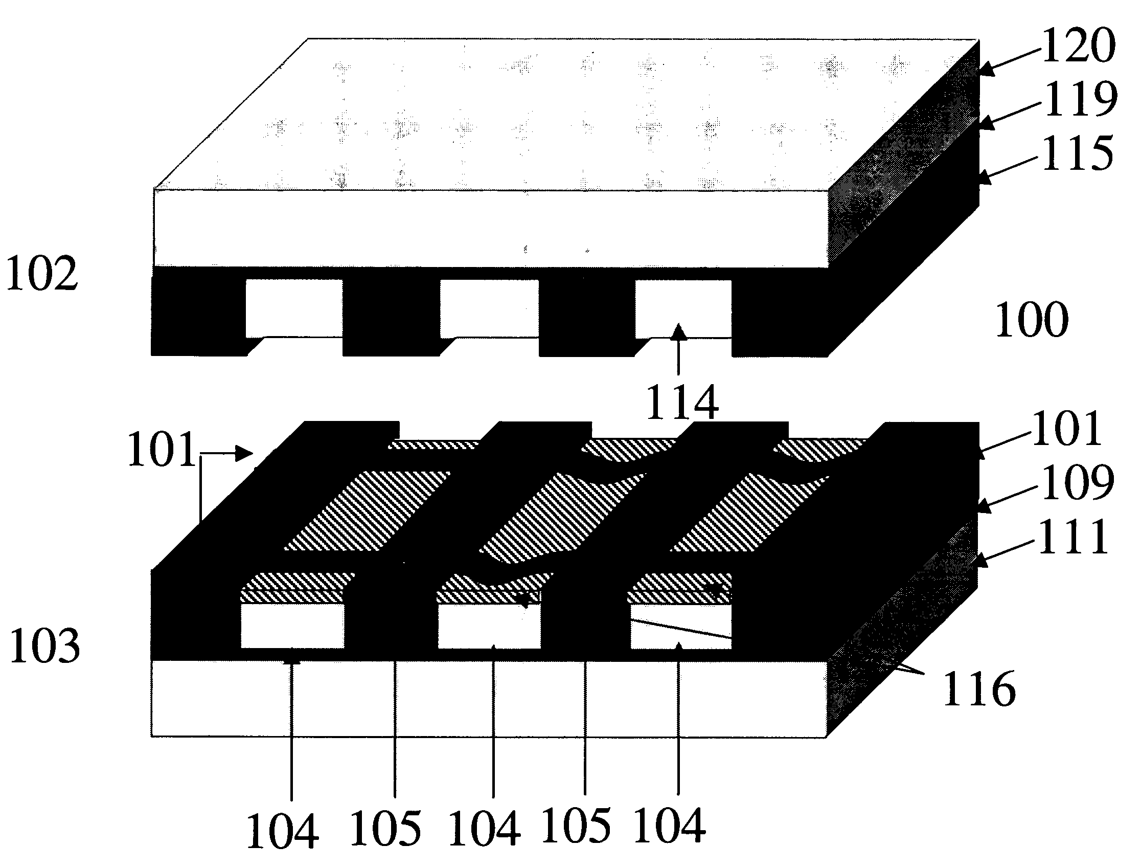
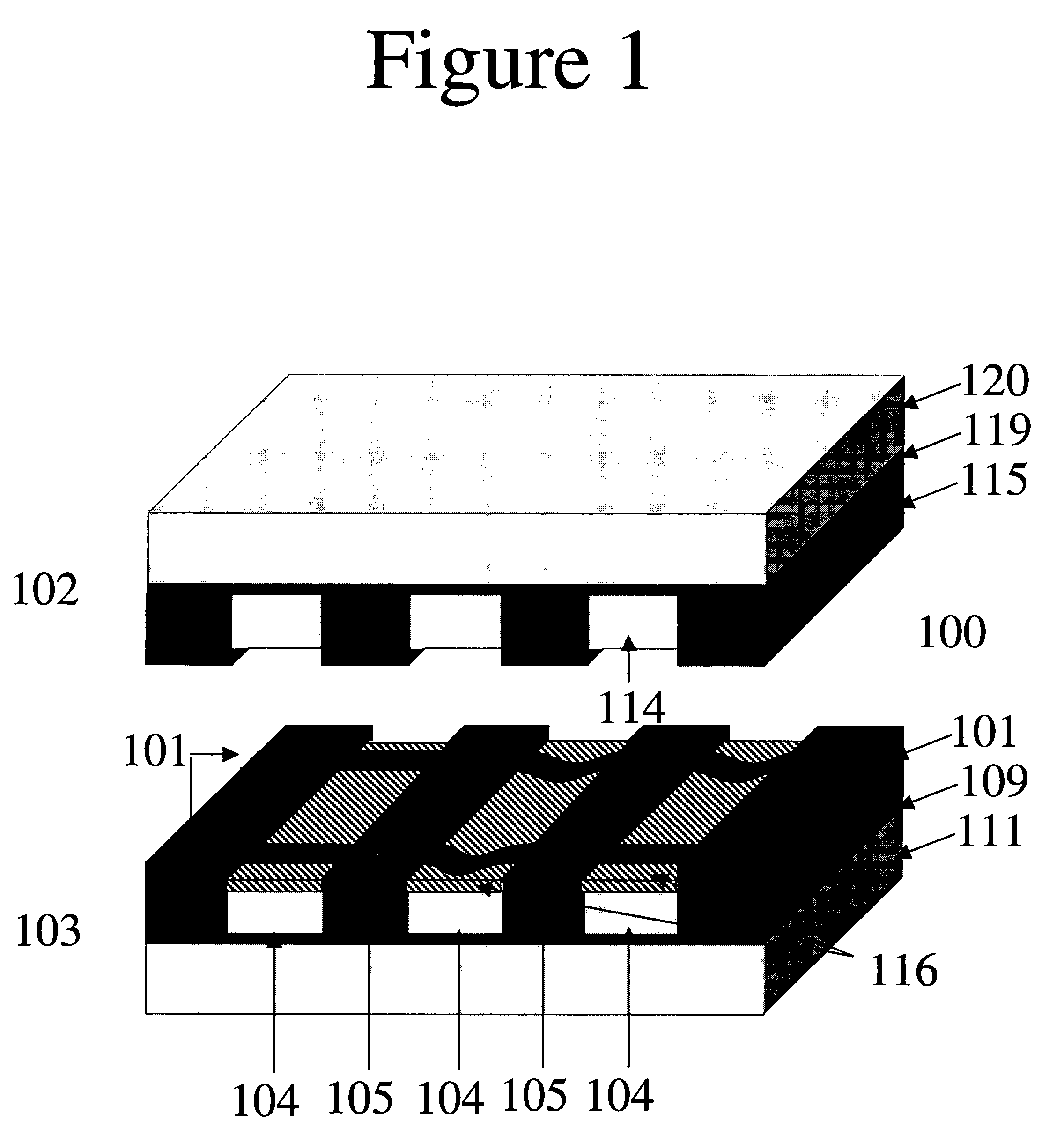
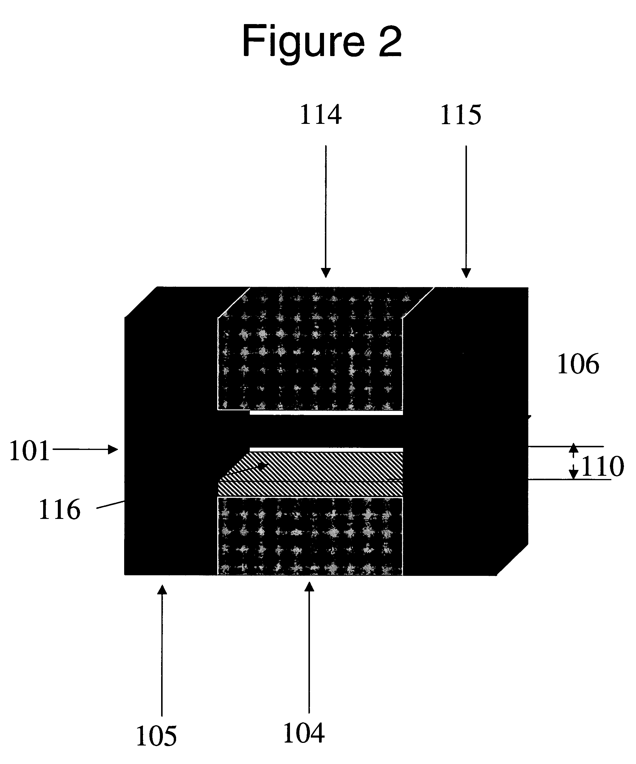
Electromechanical three-trace junction devices
a three-trace junction, electromechanical technology, applied in nanoelectromechanical switches, semiconductor/solid-state device details, instruments, etc., can solve the problems of low relative speed, power consumption, and long (millisecond) write cycles
- Summary
- Abstract
- Description
- Claims
- Application Information
AI Technical Summary
Benefits of technology
Problems solved by technology
Method used
Image

Examples
example 1
[0091]A junction with metallic traces 510 was created as described in FIG. 5 and was oxidized as follows:
[0092]Five standard cubic centimeters per minute (sccm) of O2 was flowed over an NRAM switch, ac voltage (triangle wave) was applied to the NRAM junction (5 V amplitude, 10 kHz frequency).
[0093]Amplitudes lower than 2 V are not high enough to make the switch volatile. Amplitudes higher than 7 V frequently destroy the device (very high to infinite resistance afterwards). It was found that the switch turns volatile within a few seconds of application of voltage in the presence of the O2, after which, the switch remained volatile. 5V amplitude of ac wave adequately oxidizes the electrode; however voltage amplitudes of 2 V–7 V have been successfully used for fabricating volatile devices.
PUM
 Abstract
Description
Claims
Application Information