Pixel structure with optimized subpixel sizes for emissive displays

a technology of emissive display and subpixel size, which is applied in the direction of visual presentation, instruments, semiconductor devices, etc., can solve the problems of code execution that may consume data relating to the display, and achieve the effect of optimizing the battery life and optimizing the lifetime of one or more elements of the display

Inactive Publication Date: 2007-02-13
BARCO NV
View PDF6 Cites 39 Cited by
  • Summary
  • Abstract
  • Description
  • Claims
  • Application Information

AI Technical Summary

Benefits of technology

[0015]In a further aspect the present invention provides a computer program product for carrying out any of the methods of the present invention when the computer program product is executed on a computing device. In particular, the computer program product has code segments for selecting areas of at least two sub-pixel elements of a display and modifying the areas of the at least two sub-pixel elements to optimize a lifetime of one or more elements of the display. Preferably, the computer product comprises code, when executed, which can determine the sub-pixel areas such that that each pixel element displays white at a predetermined white point within a certain tolerance. When the code is executed, the lifetimes of the sub-pixel elements may be optimized to within a predetermined tolerance of each other. Preferably the code, when executed, optimizes the sub-pixel areas so that each pixel element displays white at a predetermined white point within a certain tolerance over the lifetime of the pixel element. Preferably the code, when executed, determines the lifetime of the pixel element by the estimated brightness of the pixel element reducing to a predetermined value, e.g. in the range 40–60% of its initial value. The code, when executed can determine the lifetime of the pixel element by an estimated color shift of the pixel element greater than a predetermined value. The code, when executed, can determine the lifetime of a sub-pixel element by the estimated brightness of the sub-pixel element reducing to a predetermined value such as within a range 40–60% or 50% of its initial value. The code, when executed, can determine the lifetime of a sub-pixel element by an estimated color shift of the sub-pixel element greater than a predetermined value. Preferably, the predetermined value is a number of JND's, e.g. 3. Typically, there are at least three sub-pixels for each pixel element and the code, when executed, optimizes areas of the at least three sub-pixel elements such that the lifetimes of the sub-pixel areas are within a predetermined tolerance of each other. This predetermined tolerance may be 20%, more preferably 10%. The code when executed may consume data relating to the display, in particular performance data for pixel elements which are organic light emitting diodes. The code, when executed can calculate a temperature of each sub-pixel element when each pixel element displays white at the predetermined white point, and can calculate an aging effect on each sub-pixel element based on the calculated temperature. When the display is powered by a battery, the display element to be optimized may be the battery, and the code, when executed, may optimize the sub-pixel areas to optimize the battery lifetime between charging over the lifetime of the pixel elements.

Problems solved by technology

The code when executed may consume data relating to the display, in particular performance data for pixel elements which are organic light emitting diodes.

Method used


Image

  • Pixel structure with optimized subpixel sizes for emissive displays
  • Pixel structure with optimized subpixel sizes for emissive displays
  • Pixel structure with optimized subpixel sizes for emissive displays

Examples


Embodiment Construction

[0035]The present invention will be described with reference to certain embodiments and drawings but the present invention is not limited thereto. The skilled person will appreciate that the present invention has wide application with displays. The present invention will mainly be described with reference to OLED materials, however it may find advantageous use with a wide variety of emissive materials (both luminescent and phosphorescent materials).

[0036]In the following an emissive pixel structure refers to an emissive, fixed format pixel which may comprise a number of pixel elements, e.g. red, green and blue pixel elements. Each color element may itself be made up of one or more sub-elements. Hence, a pixel structure may comprise sub-pixel elements. A pixel structure may be monochromatic or colored. Further, the array may be a passive or active matrix.

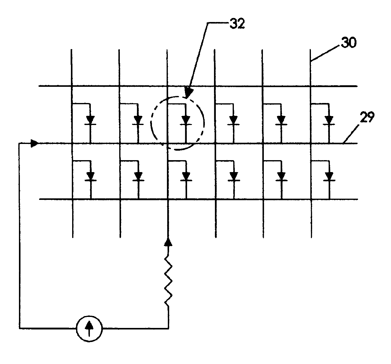
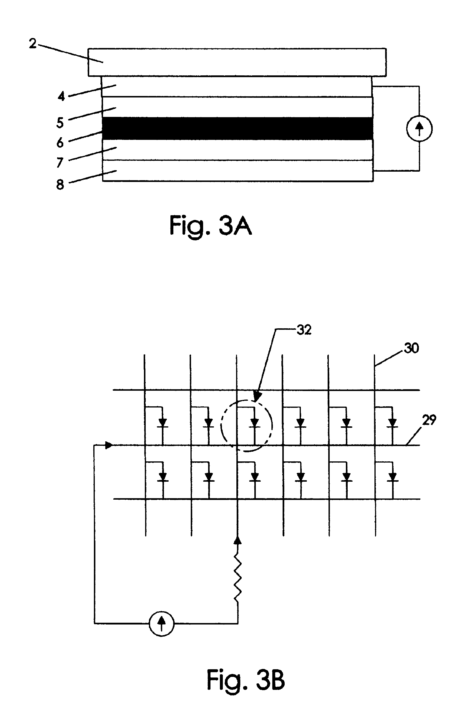
[0037]A known method of manufacture of OLED displays which may be used with the present invention results in a pixel structure as s...


PUM


Abstract

A method of designing a fixed format emissive display is described using a computing device having a processor and a memory, the display comprising an array of emissive pixel elements, each pixel element comprising at least two sub-pixel elements made of different materials. The method comprises selecting areas of the at least two sub-pixel elements so that each pixel element displays white at a predetermined white point within a certain tolerance over a lifetime of the pixel, and such that the lifetimes of the sub-pixel areas are within a predetermined tolerance of each other.A display having sub-pixel elements optimized so that each pixel element displays white at a predetermined white point within a certain tolerance over a lifetime of the pixel, and such that the lifetimes of the sub-pixel areas are within a predetermined tolerance of each other is also described.

Description

FIELD OF THE INVENTION[0001]The present invention relates to emissive displays, especially fixed format emissive displays such as flat panel displays as well as methods of designing, manufacturing and operating them. The present invention also relates to computer software for executing design methods according to the present invention on a suitable computing platform.TECHNICAL BACKGROUND[0002]Electronic displays can use transmissive or emissive materials to generate pictures or light. Emissive materials are usually phosphorescent or electroluminescent materials. Examples are inorganic electroluminescent materials such as applied in thin film and thick film electroluminescent displays (EL-displays, for example thin film TFEL displays as manufactured by Sharp, Planar, LiteArray or iFire / Westaim). Another group is organic electroluminescent materials (such as Organic Light Emitting Diode OLED material) deposited in layers comprising small molecule or polymer technology or phosphorescen...

Claims


Application Information

Patent Timeline
Patent Type & Authority Patents(United States)
IPC IPC(8): G09G3/32G09G3/22H01L27/00H01L27/32
CPCH01L27/3218Y10S345/904H10K59/353
Inventor DEDENE, NELETHIELEMANS, ROBBIEHILLE, HERBERT VANBIRD, WILLIAM E.
Owner BARCO NV
Why Eureka
Try Eureka