Display device and display method

a display device and display method technology, applied in static indicating devices, non-linear optics, instruments, etc., can solve the problems of difficult to provide a high-definition display, poor visibility of type liquid crystal display devices, and large power consumption of back-light, so as to improve light utilization efficiency, reduce brightness, and improve image quality.

Inactive Publication Date: 2007-02-13
FUJITSU LTD
View PDF5 Cites 60 Cited by
  • Summary
  • Abstract
  • Description
  • Claims
  • Application Information

AI Technical Summary

Benefits of technology

[0012]The present invention has been made with the aim of solving the above problems, and it is an object of the present invention to provide a display device and display method capable of improving the light utilization efficiency, without causing deterioration in the displayed image quality, particularly a decrease in the brightness.

Problems solved by technology

Since the reflection type liquid crystal display devices have poor visibility because the reflected light amount varies depending on environmental conditions, transmission type color liquid crystal display devices are generally used as the display devices of personal computers displaying full-color images.
For this reason, a lot of power is consumed by the back-light.
Moreover, since a color display is achieved using color filters, a single pixel needs to be composed of three sub-pixels, and there are problems that it is difficult to provide a high-definition display, and the purity of the displayed colors is not sufficient.
Similarly, in a color-filter type liquid crystal display device using a ferroelectric liquid crystal material, since the writing scanning and the erasing scanning are performed by respectively using a half of the time of each frame, there is a problem that only about a half of the light emitted by the light source is utilized for display.

Method used


Image

  • Display device and display method
  • Display device and display method
  • Display device and display method

Examples


first embodiment

[0049]FIG. 3 is a block diagram showing the circuit structure of a liquid crystal display device of the first embodiment; FIG. 4 is a schematic cross sectional view of a liquid crystal panel and a back-light; FIG. 5 is a schematic view showing an example of the overall structure of the liquid crystal display device; and FIG. 6 is an example of the structure of an LED array as a light source of the back-light.

[0050]In FIG. 3, the numerals 21 and 22 represent a liquid crystal panel and a back-light whose cross sectional structures are shown in FIG. 4. As shown in FIG. 4, the back-light 22 comprises an LED array 7 for emitting light of each of red, green and blue colors, and a light guiding / diffusing plate 6.

[0051]As shown in FIGS. 4 and 5, the liquid crystal panel 21 comprises a polarization film 1, a glass substrate 2, a common electrode 3, a glass substrate 4 and a polarization film 5, which are stacked in this order from the upper layer (front face) side to the lower layer (rear fa...

second embodiment

[0070]The following description will explain the second embodiment in which a liquid crystal material to be used and TA, TB, TC, TD are different from those in the first embodiment. Since the circuit structure and operation of the liquid crystal display device are the same as those in the first embodiment, the explanation thereof is omitted.

[0071]First, in exactly the same manner as in the first embodiment, an empty panel was fabricated. A ferroelectric liquid crystal material showing the phase sequence of isotropic phase-cholesteric phase-chiral smectic C phase from the higher temperature side and a monostable electro-optic response was sealed between the alignment films 11 and 12 of this empty panel to form a liquid crystal layer 13, and an alignment process was executed by applying a DC voltage of 10 V to the liquid crystal layer 13 in a temperature range of ±3° C. from the transition temperature to the chiral smectic C phase from the cholesteric phase (100 to 94° C.). In the ali...

third embodiment

[0080]The following description will explain the third embodiment in which the values of TA, TB, TC, TD are the same as in the first embodiment, but the ON timing of the back-light is varied. Since the circuit structure and operation of the liquid crystal display device are the same as those in the first embodiment, the explanation thereof is omitted. Besides, the structure of the liquid crystal panel, including the liquid crystal material to be used, is the same as that of the first embodiment.

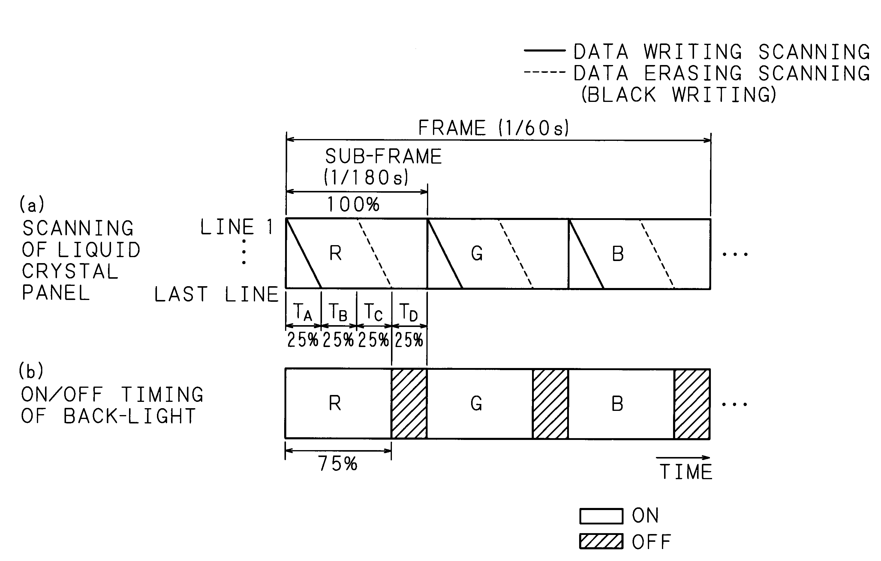
[0081]FIG. 9 shows a time chart of display control in the third embodiment, wherein FIG. 9 (a) shows the scanning timing of each line of the liquid crystal panel 21, and FIG. 9 (b) shows the ON / OFF timing of the back-light 22.

[0082]Similarly to the first embodiment, in each sub-frame obtained by dividing one frame into three sub-frames, the time (TA) necessary for data writing scanning, the time (TC) necessary for data erasing scanning, the time (TB) from the end timing of writing scanning to...


PUM

PropertyMeasurementUnit
light transmittanceaaaaaaaaaa
thickaaaaaaaaaa
particle sizeaaaaaaaaaa

Abstract

One frame is divided into three sub-frames of red, green and blue colors, and, in each sub-frame, the time (TA) necessary for writing scanning, the time (TC) necessary for erasing scanning, the time (TB) from the end timing of writing scanning to the start timing of erasing scanning, and the time (TD) from the end timing of erasing scanning to the start timing of writing scanning of the next color (the next sub-frame) are each 25% of the sub-frame. The relations TB+TC=TA+TD, and TB=TD are satisfied. A back-light is turned on during the time from the start timing of writing scanning to the end timing of erasing scanning, and is turned off during the time from the end timing of erasing scanning to the start timing of writing scanning of the next color. The ON time of the back-light is 75% of the sub-frame.

Description

BACKGROUND OF THE INVENTION[0001]The present invention relates to a field-sequential type display device and display method for performing a display by synchronizing the switching of colors of light to be incident on an optical switching element with the inputting of display data of respective colors corresponding to a display image to the optical switching element, and also relates to a color-filter type display device and display method for performing a color display by synchronizing the incidence of white light on an optical switching element having color filters with the inputting of display data of respective colors corresponding to a display image to the optical switching element.[0002]Along with the recent development of so-called information-oriented society, electronic apparatuses, such as personal computers and PDA (Personal Digital Assistants), have been widely used. With the spread of such electronic apparatuses, portable apparatuses that can be used in offices as well a...

Claims


Application Information

Patent Timeline
Patent Type & Authority Patents(United States)
IPC IPC(8): G09G3/36G02F1/133G02F1/13357G09G3/20G09G3/34
CPCG09G3/3413G02F2001/133622G09G2340/06G09G2310/061G09G2310/0235G02F1/133622G02F1/133
Inventor YOSHIHARA, TOSHIAKIMAKINO, TETSUYABETSUI, KEIICHI
Owner FUJITSU LTD
Why Eureka
Try Eureka