Oscillating circuit, booster circuit, nonvolatile memory device, and semiconductor device

a booster circuit and oscillating frequency technology, applied in pulse generators, pulse techniques, instruments, etc., can solve the problems of not being able to suppress the oscillating frequency variation of output signals, affecting the time required for charging and discharging capacitors, etc., and achieve the effect of small peak power consumption

Inactive Publication Date: 2007-02-20
TAMIRAS PER PTE LTD LLC
View PDF12 Cites 76 Cited by
  • Summary
  • Abstract
  • Description
  • Claims
  • Application Information

AI Technical Summary

Benefits of technology

[0028]In contrast, according to the arrangement of the present invention, the delay circuit includes the resistor circuit. The change in the resistances of the resistor circuit due to operating temperatures, power supply voltages are subtle, and manufacturing variations are also comparatively subtle. The change in the delay time of a resistor circuit can be made smaller compared with the change in the rising time and the fall time of the inverter. Therefore, it becomes possible to suppress the variation in the oscillating frequencies of an output signal by increasing the resistance of the resistor circuit so that the rate of the delay time of the resistor circuit to an oscillating cycle becomes large.
[0041]In the arrangement, the control section which controls the operations of the nonvolatile memory device of the present invention is provided. Here, as described above, it becomes possible to reduce the current consumption both in a steady state and during the rising of the voltage, respectively. As such, it is possible to provide a semiconductor device whose current consumption is small.

Problems solved by technology

As such, the time required for charging and discharging the capacitor is affected by the performance of the inverter which constitutes the ring oscillator.
Thus, like the conventional arrangement, when the delay circuit is constituted by a capacity, it is not possible to suppress the variation in the oscillating frequencies of the output signal due to the change in rising time and falling time of the inverter which constitutes the ring oscillator.

Method used


Image

  • Oscillating circuit, booster circuit, nonvolatile memory device, and semiconductor device
  • Oscillating circuit, booster circuit, nonvolatile memory device, and semiconductor device
  • Oscillating circuit, booster circuit, nonvolatile memory device, and semiconductor device

Examples


Embodiment Construction

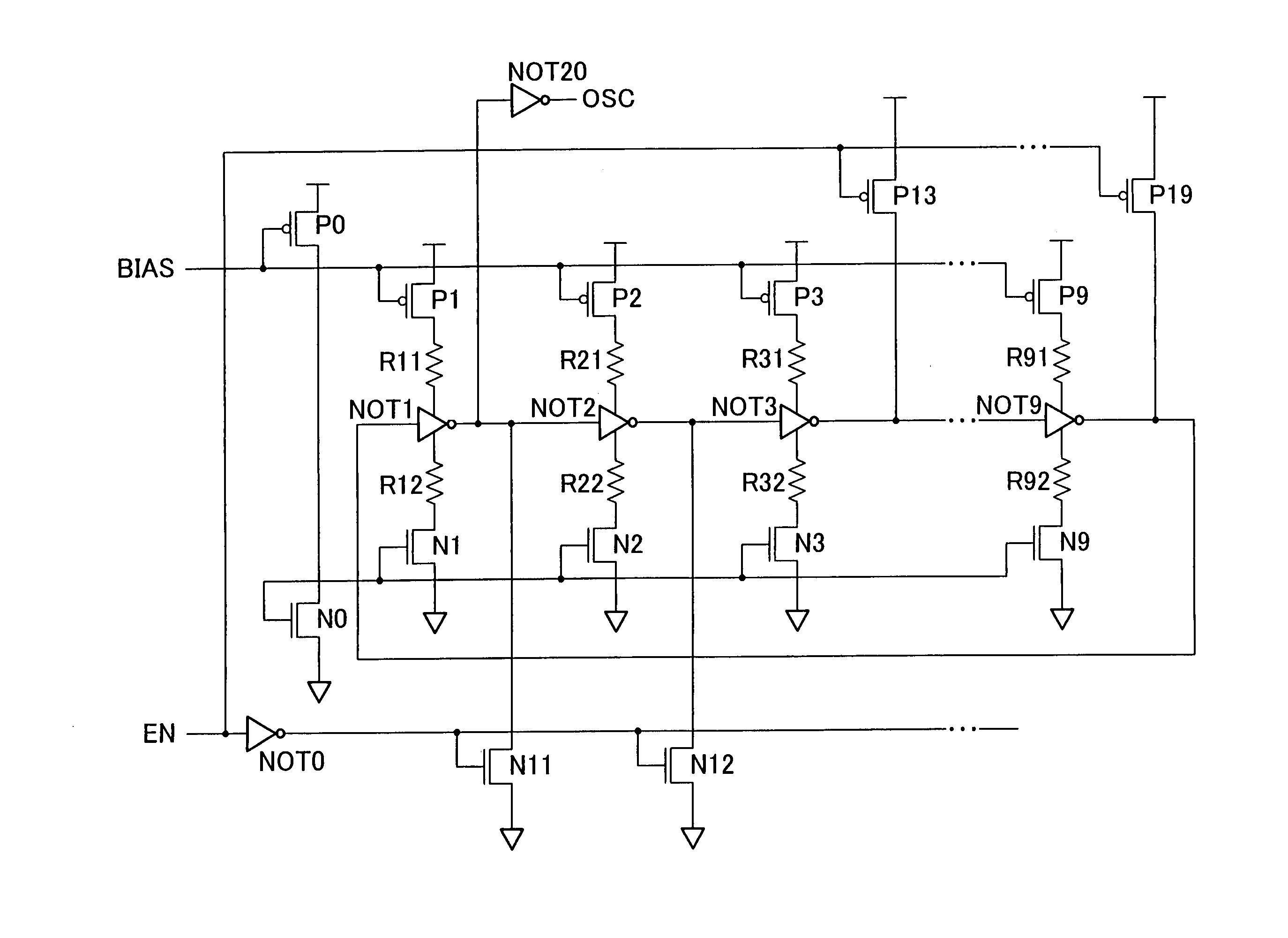
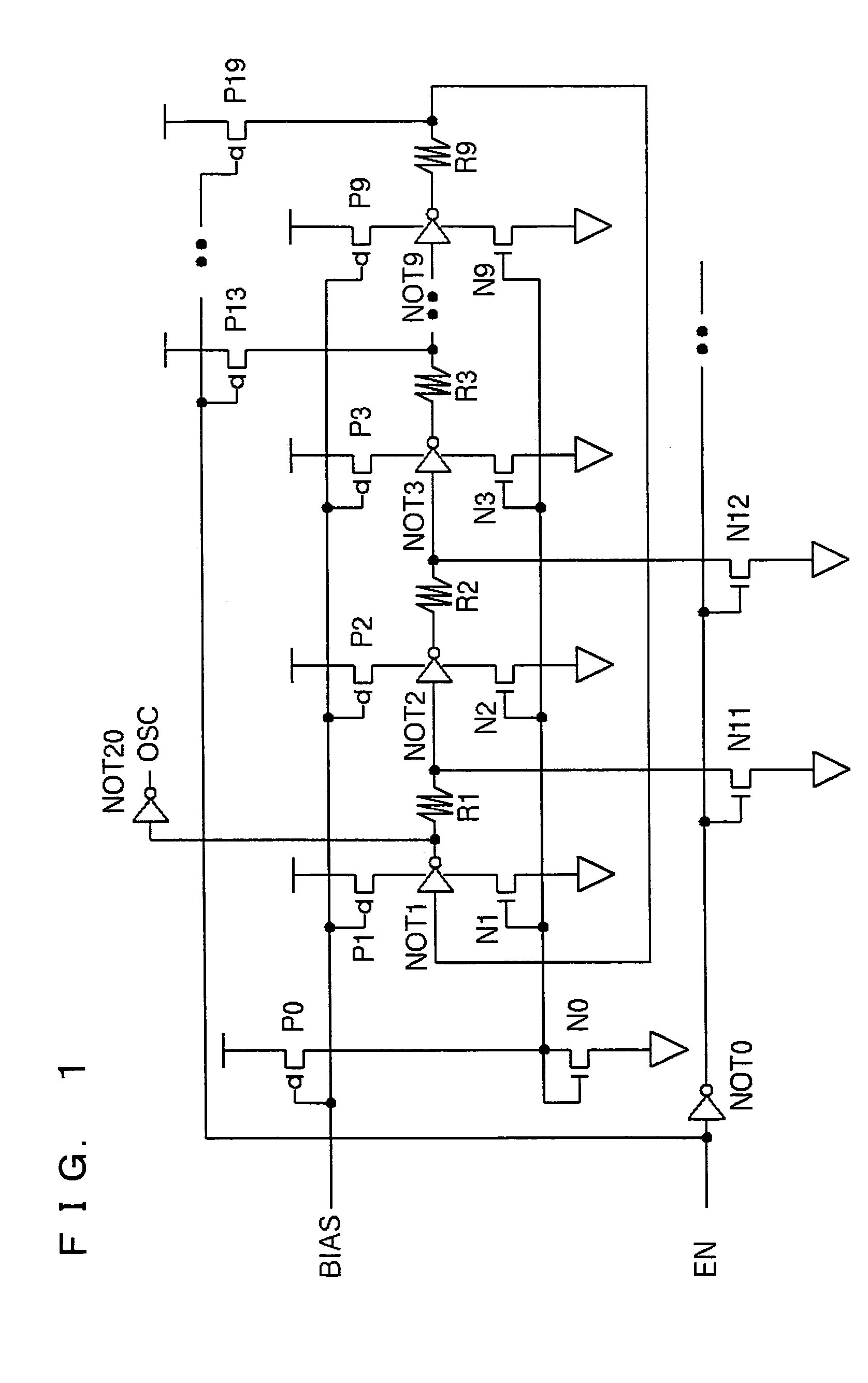
[0052]The following description deals with an embodiment of the present invention with reference to FIG. 1 through FIG. 8.

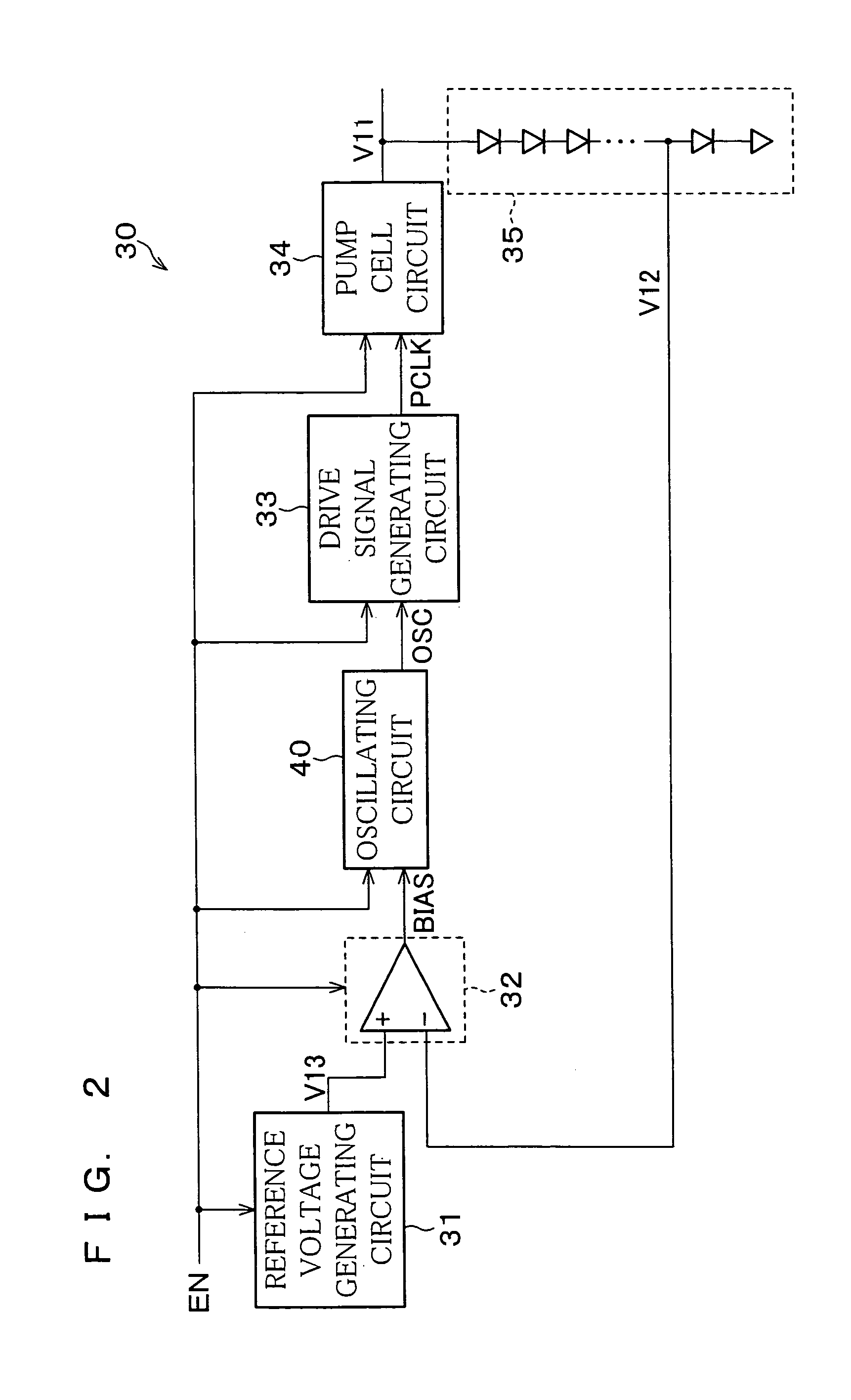
[0053]FIG. 3 shows how a flash memory of the present embodiment is arranged. As shown in FIG. 3, the flash memory is constituted by a flash macro 20, and is connected with a control circuit 11. The flash macro 20 includes a booster circuit 30, a writing / erasure voltage generating circuit 21, a row decoder 22, a column decoder 23, a flash memory cell array 24, a sense amplifier 25, an address register 26, and an input / output buffer 27.

[0054]According to need, the control circuit 11 controls the booster circuit 30, the writing / erasure voltage generating circuit 21, the row decoder 22, the column decoder 23, the sense amplifier 25, the input / output buffer 27, and the address register 26, via a control bus during read-out operation / rewriting operation.

[0055]The flash memory cell array 24 has a similar arrangement to the memory cell array shown in FIG. 5 exemplifying ...


PUM


Abstract

In a ring oscillator constituting an oscillating circuit, resistor circuits are used as delay circuits to be connected to respective inverters. That is, the inverters and the resistors are connected in series so that the resistor is provided between the adjacent inverters. With the arrangement, it is possible to provide an oscillating circuit which is less dependent on any of power supply voltages, temperatures, and manufacturing variations, while maintaining a characteristic in which the oscillating frequency decreases as an output voltage of a booster circuit increases.

Description

[0001]This application is the national phase under 35 U.S.C. § 371 of PCT International Application No. PCT / JP02 / 12574 which has an International filing date of Nov. 29, 2002, which designated the United States of America.[0002]This nonprovisional application claims priority under 35 U.S.C. § 119(a) on Patent Application No. 2001-366839 filed in JAPAN on Nov. 30, 2001, which is herein incorporated by reference.TECHNICAL FIELD[0003]The present invention relates to an oscillating circuit which controls the operation of a booster circuit for use in a nonvolatile memory device such as a flash memory.BACKGROUND ART[0004]A flash memory is one of the semiconductors which have an electrically rewritable nonvolatile memory area. The structure of a typical memory cell of the flash memory is shown in FIG. 4. This memory cell has a structure of 1 cell / 1-bit, and is composed of a control gate 51, a floating gate 52, a source 53, and a drain 54. A transistor of such a structure is called a field ...

Claims


Application Information

Patent Timeline
Patent Type & Authority Patents(United States)
IPC IPC(8): G11C7/00G11C8/00G06K19/07G11C16/06G11C5/14G11C16/02G11C16/04H03K3/011H03K3/03
CPCG11C5/145H03K3/0315H03K3/011G11C16/0416G11C5/14H01L27/04H03K3/03G11C16/30
Inventor MATSUE, KAZUKI
Owner TAMIRAS PER PTE LTD LLC
Why Eureka
Try Eureka