Method of correcting amplitude defect in multilayer film of EUVL mask

a multi-layer film and mask technology, applied in the field of mask correction, can solve the problems of large shaved foreign matter periphery and unnecessarily wide region of si film, and achieve the effect of good position controllability and reduced reflectivity

Inactive Publication Date: 2007-03-13
HITACHI HIGH TECH SCI CORP
View PDF3 Cites 15 Cited by
  • Summary
  • Abstract
  • Description
  • Claims
  • Application Information

AI Technical Summary

Benefits of technology

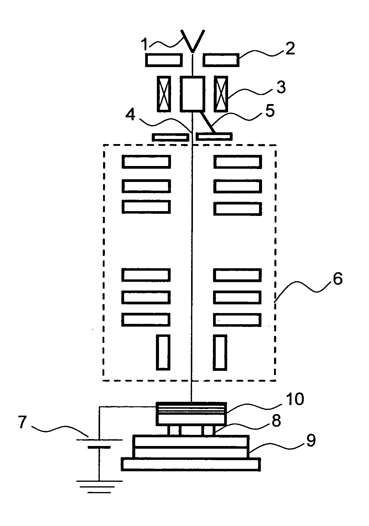
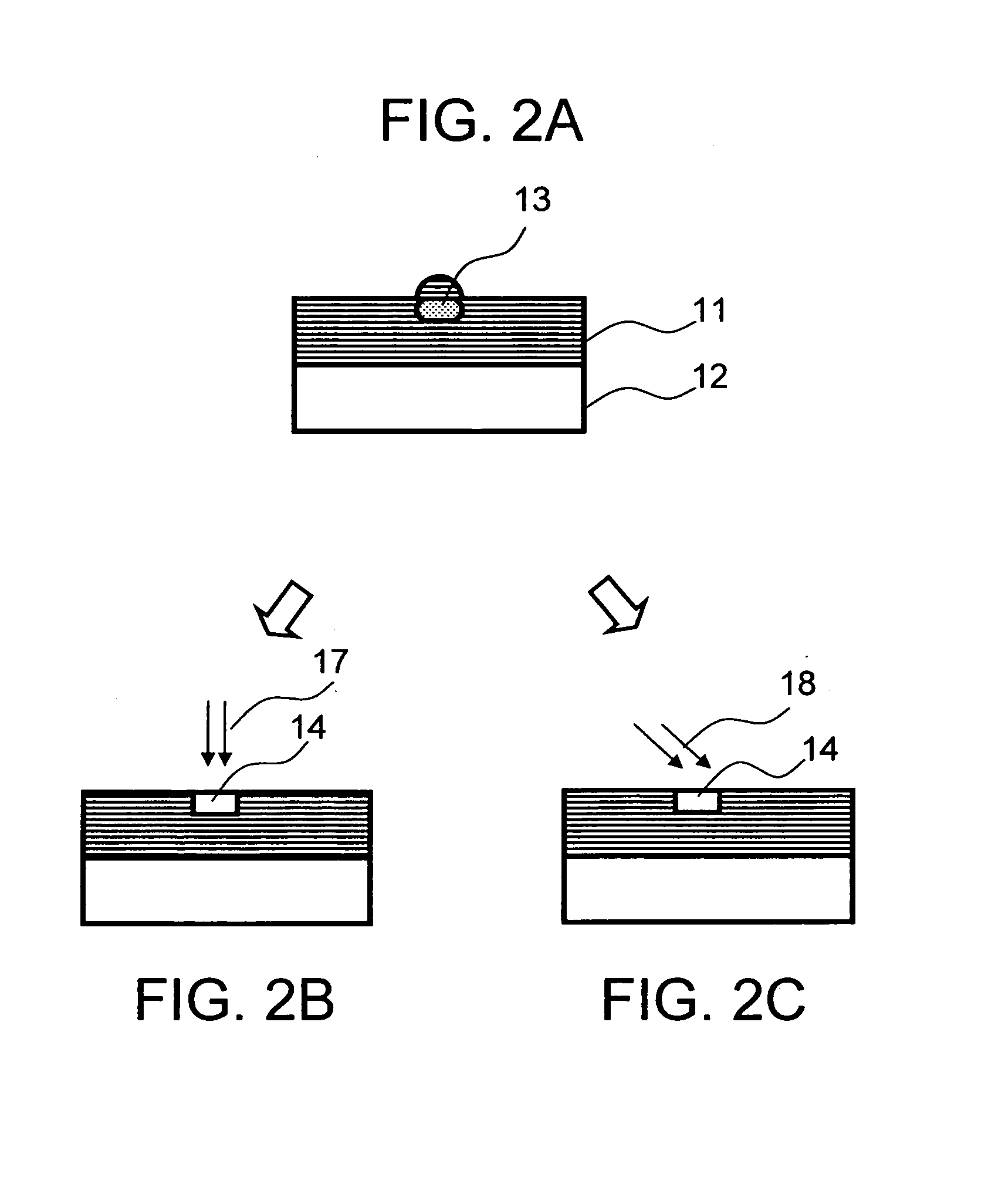
[0012]By using an apparatus having an Au—Si liquid alloy ion source, a mass separator and a focused ion optical system, an ion beam drawn out of the Au—Si liquid alloy ion source is separated only in Si by the mass separator, after having been converged by the ion optical system an Si ion beam having been decelerated to a low acceleration voltage of 500 V or lower such that an injection depth becomes less than a thickness of the multilayer film is irradiated to the Mo / Si multilayer film or the Mo2C / Si multilayer film in which the amplitude defect exists, and the multilayer film in an upper layer of a foreign matter constituting the amplitude defect and the foreign matter are removed by a physical sputter or a gas assist etching such that an interlayer of the Mo / Si multilayer film or the Mo2C / Si multilayer film in a lower layer is not destroyed.
[0013]Instead of decreasing an energy of the Si ion beam to be irradiated, the Si ion beam of 500 V–2000 V in acceleration voltage is slantingly entered such that the injection depth becomes shallow to thereby irradiate the Si ion beam to the Mo / Si multilayer film or the Mo2C / Si multilayer film in which the amplitude defect exists such that the injection depth becomes less than the thickness of the multilayer film, and the multilayer film in the upper layer of the foreign matter constituting the amplitude defect and the foreign matter are removed by the physical sputter or the gas assist etching such that the interlayer of the Mo / Si multilayer film or the Mo2C / Si multilayer film in the lower layer is not destroyed.
[0014]With respect to a place in which a step is large by removing the foreign matter, an etching is performed so as to become a Gaussian shape as a whole by removing the multilayer film around a foreign matter removal place. By doing like this, it is possible to reduce a reflectivity from being lost by a scattering at an EUV light reflection time. In order to make it the Gaussian shape, it is reduced to the low acceleration voltage of 500 V or lower, and a defocused ion beam of the Gaussian beam shape is used. By using this ion beam, shaving is collectively performed by the physical sputter or the gas assist etching. Or, an ion beam which has been converged and reduced to the low acceleration voltage of 500 V or lower is scan-irradiated, and an ion irradiation quantity is controlled in compliance with a place so as to become the Gaussian shape to thereby perform the shaving by the physical sputter or the gas assist etching.
[0015]In the above, in order to reduce the reflectivity from being lost by the scattering at the EUV light reflection time, it is desirable that the Gaussian shape is made as gentle as possible.
[0017][Advantages of the Invention] Since the Si ion beam having been decelerated to the low acceleration voltage of 500 V or lower is used in order that the injection depth becomes less than the thickness of the multilayer film, or since the amplitude defect is removed by irradiating the ion beam of 500 V–2000 V in acceleration voltage by the slanting incidence, there is no fact that the interface of the multilayer film is disarranged by the injection of the Si ion and thus the reflectivity is decreased. Further, even if the irradiated ion beam is injected into the multilayer film, since it is Si that is a light element, there is no fact that the EUV light is absorbed.
[0018]In a place in which the amplitude defect has been removed by the physical sputter, since the capping layer is formed in a vacuum intact without exposure to the air by directly depositing Si by the Si ion beam whose acceleration voltage has been decreased to single voltage to tens of volts, it is possible to surely perform the oxidation prevention of the Mo film. It is neither necessary to dispose, like a case where an Si capping layer is formed by separately using a sputter target of Si, the Si target to a suitable position near a mask, nor necessary to adjust such that sputtered Si becomes a desired position. Further, since the beam is converged in comparison with the sputter, a position controllability is good as well.

Problems solved by technology

In the above proposed method of correcting the amplitude defect of the Mo / Si multilayer film (or Mo2C / Si multilayer film), although the Ar ion beam of 500 V is used, since a gas ion source is large in its light source size and additionally used in the low acceleration, it is impossible to converge the ion beam, so that there has been a problem that a foreign matter periphery is widely shaved.
Further, there have been problems that, in order to film-form the capping layer, it is necessary to dispose an Si target for the sputter to a suitable position near the mask, additionally it is also necessary to adjust sputtered Si so as to be deposited to a desired position, and further an Si film is adhered to an unnecessarily wide region because it is a sputter film.

Method used


Image

  • Method of correcting amplitude defect in multilayer film of EUVL mask
  • Method of correcting amplitude defect in multilayer film of EUVL mask
  • Method of correcting amplitude defect in multilayer film of EUVL mask

Examples


Embodiment Construction

[0023]Hereunder, it is explained about an embodiment of the present invention by referring to the drawings.

[0024]FIG. 1 is a schematic sectional view of a focused ion beam apparatus used in the present invention.

[0025]After film-forming the Mo / Si multilayer film (or Mo2C / Si multilayer film), an EUVL mask 10, in which there has been found, by a survey instrument, the amplitude defect which has been made by the fact that the foreign matter is mixed to a vicinity of the multilayer film surface and decreases the intensity of EUV reflected light, is introduced into a vacuum apparatus having an AU—Si liquid alloy ion source 1, a mass separator 3, a focused ion optical system 6 and a high accuracy XY stage 9, and the XY stage 9 is moved such that a position in which the amplitude defect has been found comes to a visual field center. An electrode is formed in an end part of the Mo / Si multilayer film (or Mo2C / Si multilayer film) so as to be capable of intending to decrease an acceleration vo...


PUM

PropertyMeasurementUnit
voltageaaaaaaaaaa
angleaaaaaaaaaa
wavelengthaaaaaaaaaa

Abstract

By entering a low acceleration Si ion beam of 500 V or lower or a low acceleration Si ion beam of 500 V-2000 V having been slanted such that an injection depth becomes shallow, which has been mass-separated from a liquid alloy ion source containing Si by a mass separator and converged by an ion optical system, the amplitude defect near a surface of the Mo / Si multilayer film or the Mo2C / Si multilayer film is removed by a physical sputter or a gas assist etching such that an interlayer of the Mo / Si multilayer film or the Mo2C / Si multilayer film in a lower layer is not destroyed.

Description

[0001]This application claims priority under 35 U.S.C. § 119 to Japanese Patent Application No. 2004-236941 filed Aug. 17, 2004, the entire content of which is hereby incorporated by reference.BACKGROUND OF THE INVENTION[0002]The present invention relates to a method of correcting an amplitude defect of an Mo / Si multilayer film or an Mo2C / Si multilayer film of an EUVL mask by a focused ion beam.[0003]At present, an optical projection exposure apparatus using KrF of wavelength 248 nm or an ArF eximer laser of wavelength 193 nm is used in a pattern transcription to a wafer. Recently, there is reported a possibility of capable of dealing with till 65 nm rule or 45 nm rule in half pitch by using in combination a liquid immersion technique in which a resolving power is improved by filling between an objective lens of the projection exposure apparatus and the wafer with a medium of high refractive index and an ultra-resolution technique such as deformation illumination and Levenson-type p...

Claims


Application Information

Patent Timeline
Patent Type & Authority Patents(United States)
IPC IPC(8): H01L21/302G03F1/24G03F1/72G03F1/74H01L21/027
CPCB82Y10/00G03F1/74B82Y40/00G03F1/24
Inventor TAKAOKA, OSAMU
Owner HITACHI HIGH TECH SCI CORP
Why Eureka
Try Eureka