Data writing apparatus, data writing method, and program

a data writing apparatus and data technology, applied in error detection/correction, memory adressing/allocation/relocation, instruments, etc., can solve the problems of inability to write correctly, large ratio of defective memory blocks (memory blocks which cannot store data correctly), and high cost of nand type flash memory,

Inactive Publication Date: 2007-03-13
TOKYO ELECTRON DEVICE
View PDF9 Cites 15 Cited by
  • Summary
  • Abstract
  • Description
  • Claims
  • Application Information

AI Technical Summary

Benefits of technology

[0010]Accordingly, an object of the present invention is to provide a data writing apparatus, a data writing method, and a program for writing same data efficiently in a plurality of storage devices which might have defective memory blocks.
[0020]According to this invention, since a memory block in which data is to be written is designated based on error information, it is possible to write same data efficiently in a plurality of storage devices which might have defective memory blocks.

Problems solved by technology

However, when compared to NAND type and AND type flash memories, NOR type flash memories are expensive and have low integrated density.
However, the ratios of defective memory blocks (memory blocks which cannot store data correctly) included in all the memory blocks constituting the memory areas of the NAND type and AND type flash memories are intolerably large.
Accordingly, in many cases, when addressing a plurality of NAND type (or AND type) flash memories in parallel to write same data, writing cannot be correctly performed.
However, the above method is inefficient, and if NAND type (or AND type) flash memories in which data is to be written are existing in a large number, quite a long time is required to complete writing.
Therefore, it has been quite difficult to mass produce products including NAND type (or AND type) flash memories in which predetermined data is preinstalled.

Method used


Image

  • Data writing apparatus, data writing method, and program
  • Data writing apparatus, data writing method, and program
  • Data writing apparatus, data writing method, and program

Examples


first embodiment

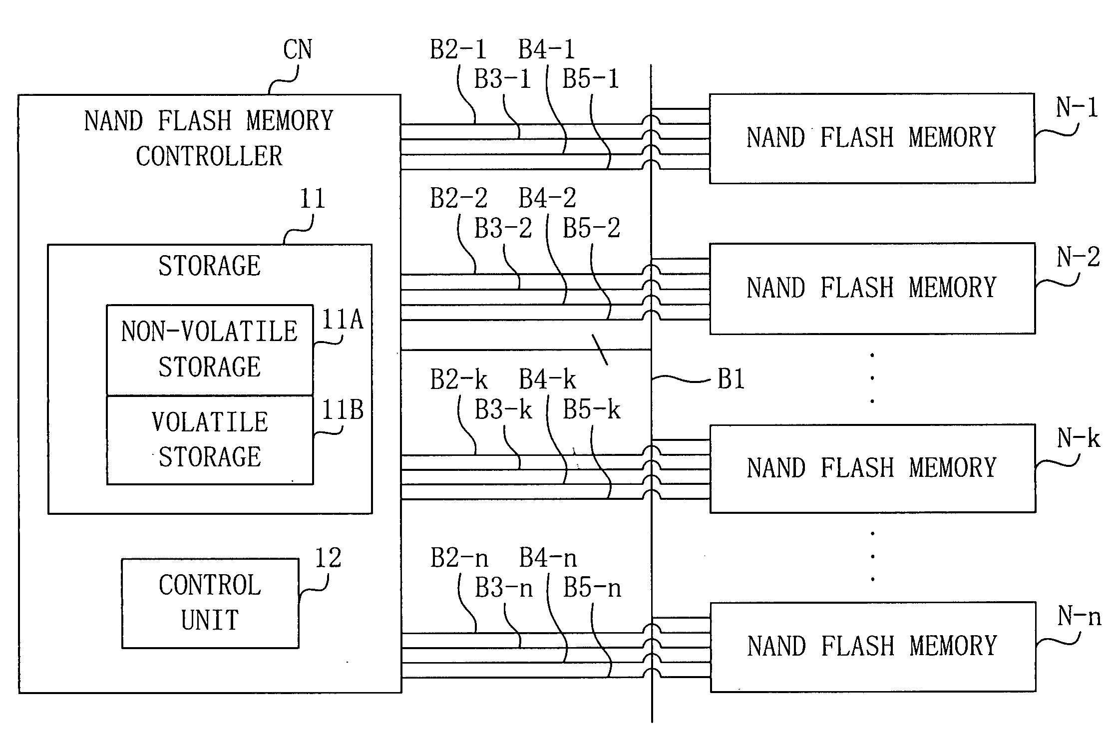
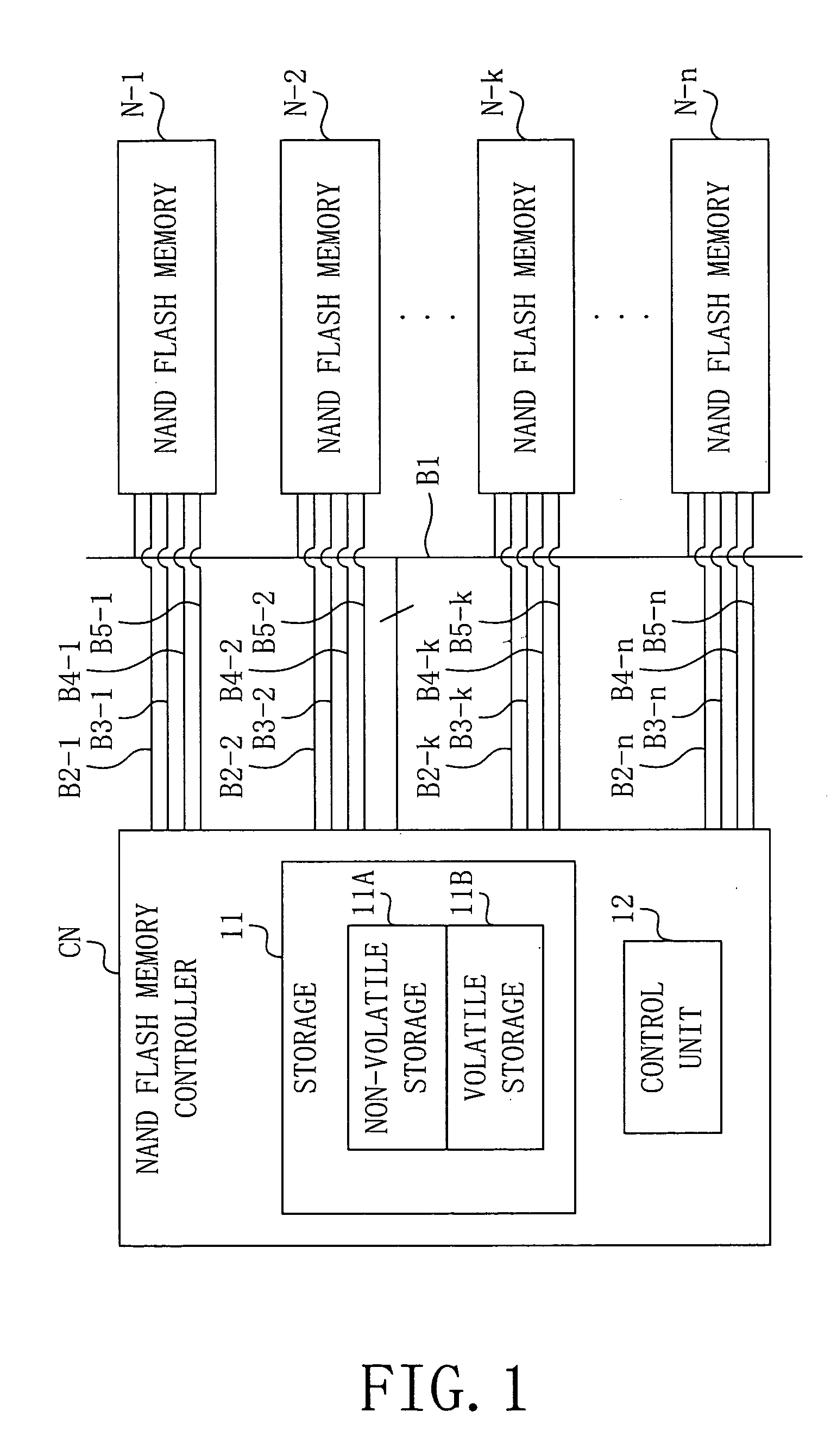
[0071]A flash memory writing apparatus according to a fist embodiment has a structure shown in FIG. 1, and writes same data in a n (n is an integer equal to or greater than 2) number of NAND flash memories N−1 to N-n.

[0072]As shown in FIG. 1, the flash memory writing apparatus according the first embodiment comprises a NAND flash memory controller (memory controller) CN, a bus B1, address latch enable (ALE) signal lines B2-1 to B2-n, command latch enable (CLE) signal lines B3-1 to B3-n, read enable (RE) signal lines B4-1 to B4-n, and ready signal lines B5-1 to B5-n.

[0073]The memory controller CN is connected to the NAND flash memories N−1 to N-n equally through the bus B1. The bus B1 is constituted by a data / address bus having a bit width of plural bits, and a write enable (WE) signal line.

[0074]Further, the memory controller CN is connected to the NAND flash memories N−1 to N-n separately through the ALE signal lines B2-1 to B2-n, the CLE signal lines B3-1 to B3-n, the RE signal li...

second embodiment

[0221]Next, a flash memory writing apparatus according to a second embodiment of the present invention will now be explained with reference to the drawings.

[0222]As shown in FIG. 12, the flash memory writing apparatus according to the second embodiment comprises a NAND flash memory controller (memory controller) CN, read enable (RE) signal lines B4-1 to B4-n, ready (R) signal lines B5-1 to B5-n, write enable (WE) signal lines B6-1 to B6-n, and a bus B7.

[0223]The RE signal line B4-k (k is an integer equal to or greater than 1 and equal to or smaller than n) is connected to a RE terminal of a NAND flash memory N-k.

[0224]The ready signal line B5-k is connected to a ready terminal of the NAND flash memory N-k.

[0225]The WE signal line B6-k is connected to a WE terminal of the NAND flash memory N-k.

[0226]The bus B7 comprises a data / address bus, an address latch enable (ALE) signal line, and a command latch enable (CLE) signal line.

[0227]The data / address bus is connected to data / address bu...


PUM


Abstract

Each of a plurality of storage devices (N−1 to N-n) has a plurality of memory blocks for storing data. A data writing apparatus obtains error information which represents good blocks which can store data correctly, from the plurality of storage devices (N−1 to N-n). The data writing apparatus determines a memory block in which data is to be written, in each of the plurality of storage devices (N−1 to N-n), based on the obtained error information. The data writing apparatus controls the plurality of storage devices (N−1 to N-n), and writes predetermined data in the determined memory blocks.

Description

TECHNICAL FIELD[0001]The present invention relates to an apparatus, a method, and a program for writing data in a storage device. Particularly, the present invention relates to an apparatus, a method and a program for writing same data into a plurality of storage devices.BACKGROUND ART[0002]Flash memories known as small-sized storage devices are roughly classified into NOR type, NAND type, and AND type.[0003]NOR type flash memories can be randomly accessed on a basis of one byte unit. However, when compared to NAND type and AND type flash memories, NOR type flash memories are expensive and have low integrated density.[0004]On the other hand, since NAND type and AND type flash memories are low-cost and have high integrated density when compared to NOR type flash memories, those flash memories are widely used. For example, TH58512FT (TOSHIBA) is known as one of AND type flash memories.[0005]However, the ratios of defective memory blocks (memory blocks which cannot store data correctly...

Claims


Application Information

Patent Timeline
Patent Type & Authority Patents(United States)
IPC IPC(8): G06F13/00G06F12/16G11C16/02G11C16/04G11C16/10G11C29/00
CPCG11C16/102G11C29/883G11C29/88G11C16/0483G11C29/76
Inventor YOSHII, TAKEOSHIMIZU, MASAHIKO
Owner TOKYO ELECTRON DEVICE
Why Eureka
Try Eureka