Semiconductor laser apparatus

a laser and semiconductor technology, applied in the direction of laser details, laser optical resonator construction, optical resonator shape and construction, etc., can solve the problem of not being able to apply immediately to a variety of purposes

Inactive Publication Date: 2007-03-27
HAMAMATSU PHOTONICS KK
View PDF13 Cites 2 Cited by
  • Summary
  • Abstract
  • Description
  • Claims
  • Application Information

AI Technical Summary

Benefits of technology

[0007]That is, irrespective of a laser diode itself of small size, a conventional semiconductor laser apparatus includes an optical element in addition to the laser diode, resulting in an enlarged apparatus size. In particular, in the cases of a laser diode array and a laser diode array stack that are integrated in a state that plural laser diodes are arranged in an array, the apparatus size of the semiconductor laser apparatus is further enlarged.
[0008]The present invention is made to overcome the aforementioned problems, and it is an object to provide a semiconductor laser apparatus capable of reducing a spread angle of an emission light with downsizing.
[0013]More specifically, it is preferable that in a region of the active region through which light totally reflected at a reflection angle of zero degree by the first reflection structure, among the light reaches to the second reflection structure, passes, the region has a shape such that a sectional area on the second end surface side is narrower than that on the first end surface side. In this case, a vertical resonance between the first reflection structure and second reflection structure is suppressed, and a laser resonance between the first reflection structure and partial reflection structure is produced efficiently. As a result, the power of the laser beam outputted from the partial reflection structure is intensified.
[0014]On the other hand, in a region of the active region through which light reflected at a reflection angle of zero degree by the partial reflection structure, among the light reaches to the second reflection structure, passes, the region may have a shape such that a sectional area on the second end surface side is narrower than that on the first end surface side. Also, in this case, a vertical resonance between the partial reflection structure and second reflection structure is suppressed, and a laser resonance between the first reflection structure and partial reflection structure is produced efficiently. As a result, the power of the laser beam outputted from the partial reflection structure is intensified.

Problems solved by technology

Since such a laser beam outputted from the laser diode has a large spread angle, it cannot be immediately applied to a variety of purposes.

Method used


Image

  • Semiconductor laser apparatus
  • Semiconductor laser apparatus
  • Semiconductor laser apparatus

Examples


first embodiment

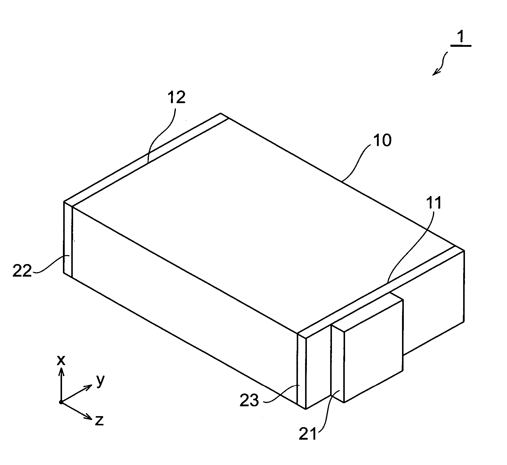
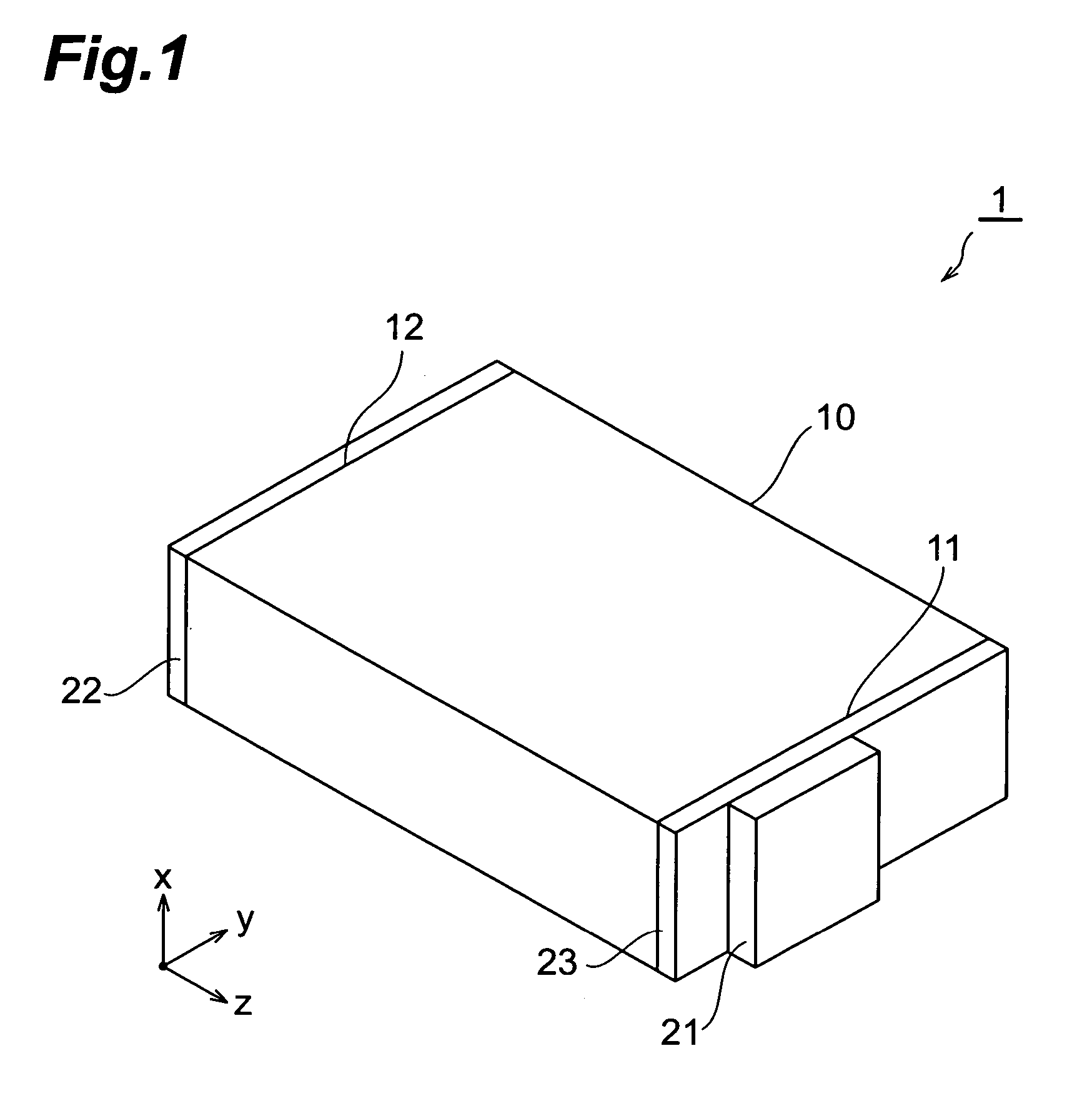
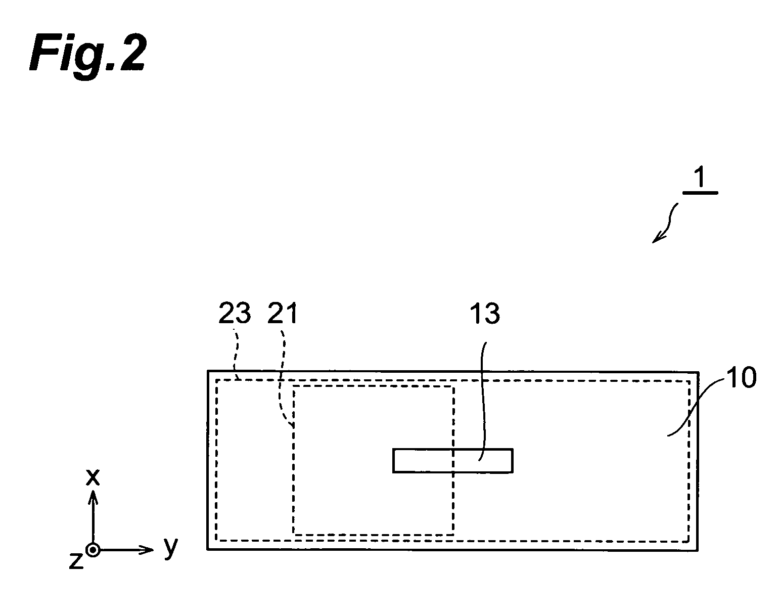
[0030]A first embodiment of a semiconductor laser apparatus according to the present invention will be first explained below. FIG. 1 is a perspective view showing a construction of the first embodiment of the semiconductor laser apparatus according to the present invention. FIG. 2 is a front view showing the construction of the first embodiment of the semiconductor laser apparatus according to the present invention. FIG. 3 is a cross-sectional view showing the construction of the first embodiment of the semiconductor laser apparatus according to the present invention.

[0031]A semiconductor laser apparatus 1 according to the first embodiment includes a semiconductor light-emitting device 10 having a light emitting active region 13 between a first end surface 11 and a second end surface 12 facing each other. A first reflection film 21 included in a first reflection structure and a partial reflection film 23 included in a partial reflection structure are formed on the side of the first ...

second embodiment

[0038]A second embodiment of the semiconductor laser apparatus according to the present invention will be next explained below. FIG. 4 is a cross-sectional view showing a construction of the second embodiment of the semiconductor laser apparatus according to the present invention. Note that the appearance of a semiconductor laser apparatus 2 according to the second embodiment is similar to that of the semiconductor laser apparatus 1 according to the foregoing first embodiment (see FIGS. 1 and 2).

[0039]As shown in FIG. 4, at a first end surface 11 a portion overlapping with an active region 13 in a first reflection film 21 constitutes a first total reflection region 31, while a portion not overlapping with the first reflection film 21 in a partial reflection film 23 constitutes a partial reflection region 33. At a second end surface 12 a portion overlapping with the active region 13 in a second reflection region 22 constitutes a second total reflection region 32.

[0040]At the semicond...

third embodiment

[0043]A third embodiment of the semiconductor laser apparatus according to the present invention will be next explained below. FIG. 5 is a cross-sectional view showing a construction of the third embodiment of the semiconductor laser apparatus according to the present invention. Note that the appearance of a semiconductor laser apparatus 3 according to the third embodiment is similar to that of the semiconductor laser apparatus 1 according to the aforementioned first embodiment (see FIGS. 1 and 2).

[0044]As shown in FIG. 5, at a first end surface 11 a portion overlapping with an active region 13 in a first reflection film 21 constitutes a first total reflection region 31, while a portion not overlapping with the first reflection region 21 in a partial reflection film 23 constitutes a partial reflection region 33. At a second end surface 12 a portion overlapping with the active region 13 in a second reflection region 22 constitutes a second total reflection region 32.

[0045]At the semi...


PUM


Abstract

A semiconductor laser apparatus capable of reducing a spread angle of emission light with downsizing has an active region between first and second end surfaces. A first reflection structure and a partial reflection structure are provided on the first end surface side. The end surface of the active region is divided into a total reflection region and a partial reflection region in combination with the first reflection structure and partial reflection structure. A laser resonator includes the first reflection structure and partial reflection structure. A second reflection structure is positioned on the way of a resonance optical path of the laser resonator. Light emitted within the active region propagates on a resonance optical path. An induction emission is produced. The semiconductor laser carries out a laser oscillation. Of the light arriving at the partial reflection structure, the portion transmitted through the partial reflection structure is outputted outside the apparatus.

Description

BACKGROUND OF THE INVENTION[0001]1. Field of the Invention[0002]The present invention relates to a semiconductor laser apparatus including an active region that emits light having a predetermined wavelength as a semiconductor light-emitting device.[0003]2. Related Background Art[0004]A laser diode that is a semiconductor light-emitting element has a light-emitting active region between a first end surface and a second end surface facing each other. A partial reflection film is formed on the first surface side, while a total reflection film is formed on the first end surface side. A laser resonator is constituted between these partial and total reflection films. Namely, the light emitted in the active region is totally reflected at the total reflection film, and partially reflected at the partial reflection film. The emitted light goes and returns in the laser resonator constructed by these partial and total reflection films, and at this time an induction emission is produced. Thus, ...

Claims


Application Information

Patent Timeline
Patent Type & Authority Patents(United States)
IPC IPC(8): H01S5/00H01S3/08H01S3/082H01S5/028H01S5/10H01S5/40
CPCH01S5/1082H01S5/4031H01S5/0286H01S2301/18H01S5/1089
Inventor GAO, XINZHENG, YUJIN
Owner HAMAMATSU PHOTONICS KK
Why Eureka
Try Eureka