Semiconductor memory and burn-in test method of semiconductor memory

a technology of semiconductor memory and burn-in test method, which is applied in the direction of information storage, static storage, digital storage, etc., can solve the problems of increased parasitic capacitance, increased parasitic capacitance, and increase of coupling capacitance between the wiring lines, so as to achieve the effect of reducing the number of circuits to be formed within the semiconductor memory for burn-in test, reducing the number of circuits to be burned in, and reducing the number of burn-in tests

Inactive Publication Date: 2007-04-03
SOCIONEXT INC
View PDF8 Cites 19 Cited by
  • Summary
  • Abstract
  • Description
  • Claims
  • Application Information

AI Technical Summary

Benefits of technology

[0011]It is an object of the invention to optimize a voltage pattern applied to a bit line during a burn-in test for the bit line, so as to reduce the burn-in test time.
[0014]The voltages are applied to the bit line pairs for the same lengths of time in each of the first to sixth steps. Stress is applied between all adjacent bit lines for the same length of time in each of the first to sixth steps. Since there is no deviation in the lengths of time that the stress is applied to the bit lines, there are no bit lines to which the stress is excessively applied. Accordingly, it is possible to prevent characteristics of memory cells from excessively deteriorating due to the burn-in test. Also, in the first to sixth steps, it is possible to minimize the number of bit lines to which the stress is not applied. Accordingly, it is possible to increase the ratio (burn-in efficiency) of bit lines to which the stress is applied, which causes burn-in time to be reduced. As a result, it is possible to reduce the test cost.
[0017]Accordingly, in the burn-in test of a semiconductor memory, it is possible to switch between the first burn-in test in which different voltage levels are applied to the bit line pairs and the second burn-in test in which different voltage levels are applied to adjacent bit line pairs, thereby efficiently performing the burn-in test. Accordingly, it is possible to increase the ratio (burn-in efficiency) of the bit lines to which stress is applied, causing burn-in time to be reduced. As a result, it is possible to reduce the test cost. Also, since it is possible to eliminate deviation in the lengths of time that the stress is applied between the bit lines, it is possible to prevent characteristics of memory cells from excessively deteriorating due to the burn-in test.
[0021]Furthermore, according to a preferred example in the first and second aspects of the present invention, when the illegal command and the test code indicate an entry command to shift to the first burn-in test mode, a write operation is performed by the operation control circuit in response to the entry command. For example, the write data is generated by the pattern generator in the data input / output circuit. The pattern generator generates data to be written to the bit lines and the memory cells according to the pattern selection signal. When the illegal command and the test code indicate an entry command to shift to the second burn-in test mode, each of the first and second precharge voltage lines are set to one or the other of high and low voltage levels according to the value of the test code. By using circuits which perform a write operation according to a performed test, the number of circuits to be formed within the semiconductor memory for the burn-in test can be minimal.
[0022]In addition, according to a preferred example in the first and second aspects of the present invention, when the illegal command and the test code received during the first and second burn-in test modes indicate an exit command, an operation mode shifts from the first and second burn-in test modes to the normal operation mode. By applying a common exit command to all the test modes, it is possible to easily return the semiconductor memory to the normal operation mode regardless of the test mode.
[0023]Further, according to a preferred example in the second aspect of the present invention, the command decoder outputs a first or second burn-in test signal to set an operation mode to the first or second burn-in test mode according to the test signal received by the test pad. When the test signal indicates the first burn-in test, the command decoder outputs a write signal to perform a write operation on the memory cell in synchronization with the test signal, and outputs a pattern selection signal. The pattern generator generates data to be written to the bit lines and the memory cells according to the pattern selection signal. The precharge voltage generator operates according to the second burn-in test signal. The reset selection part, the sense amplifier selection part, and the column selection part operate according to the write signal and the first and second burn-in test signals. Accordingly, it is possible to automatically perform the first burn-in test in the semiconductor memory without the need to receive an access command from the outside. Accordingly, it is possible to perform the first and second burn-in tests even when there are no expensive test apparatus. That is, it is possible to efficiently perform a burn-in test according to the test environment.

Problems solved by technology

However, if the distance between adjacent wiring lines is reduced due to the minute size of the device structures, the coupling capacitance between the wiring lines will increase.
For example, operation characteristics of DRAMs deteriorate by increased parasitic capacitance between bit lines connected to memory cells.
As a result, burn-in test time increases, which causes the test cost to increase.

Method used


Image

  • Semiconductor memory and burn-in test method of semiconductor memory
  • Semiconductor memory and burn-in test method of semiconductor memory
  • Semiconductor memory and burn-in test method of semiconductor memory

Examples


Embodiment Construction

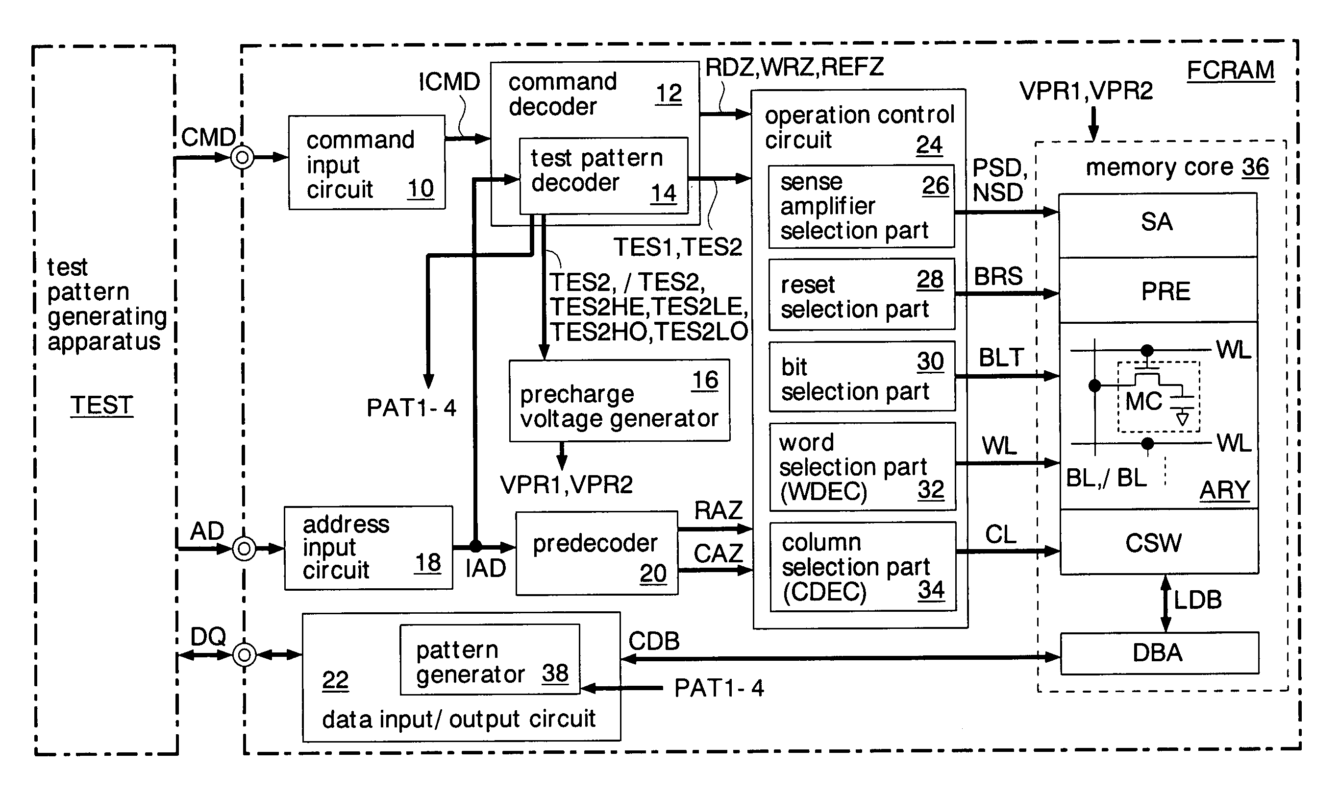
[0039]Preferred embodiments of the invention will now be described with reference to the accompanying drawings. In the drawings, double circles denote an external terminal, and a bold signal line denotes a plurality of signal lines. A part of a block connected to a bold line is composed of a plurality of circuits. A signal line through which a signal is transferred is denoted by a symbol equal to the name of the signal. A signal suffixed with ‘ / ’ indicates a negative logic. A signal prefixed with ‘Z’ indicates a positive logic.

[0040]FIG. 1 is a block diagram illustrating a semiconductor memory according to a first embodiment of the invention. The semiconductor memory is an FCRAM (Fast Cycle RAM) that has memory cells (dynamic memory cells) of a DRAM and an interface of an SRAM using a CMOS technology. The FCRAM is a kind of pseudo SRAM. The FCRAM performs a refresh operation inside a chip at regular intervals instead of receiving a refresh command from the outside, thereby maintaini...


PUM


Abstract

A burn-in test, including first to sixth steps where voltages are applied for the same lengths of time in each step, is applied to a semiconductor memory having alternately arranged bit line pairs with twist structure where the bit lines cross each other and bit line pairs with non-twist structure where the bit lines are parallel to each other. Since lengths of time in which a stress is applied for all bit lines can be equally set, no deviation occurs in lengths of time where stress is applied between the bit lines. Characteristics of memory cells can be prevented from excessively deteriorating from the burn-in test. Further, the number of bit lines not having stress applied can be minimized in the first to sixth steps. Accordingly, the ratio of the bit lines having stress applied can be increased, which reduces the burn-in test time. Thus, test cost can be reduced.

Description

CROSS REFERENCE TO RELATED APPLICATION[0001]This application is based upon and claims the benefit of priority from Japanese Patent Application No. 2005-187389, filed on Jun. 27, 2005, the entire contents of which are incorporated herein by reference.BACKGROUND OF THE INVENTION[0002]1. Field of the Invention[0003]The present invention relates to a burn-in test method of a semiconductor memory having a bit line twist structure in which bit lines cross each other.[0004]2. Description of the Related Art[0005]Semiconductor memories such as DRAMs have been used as work memories for portable equipments such as mobile phones. In recent years, mobile phones allow users to send character-string data or image data and to access the Internet in addition to allowing the users to make voice communications. The amount of data processed by mobile phones is tending to significantly increase. Accordingly, semiconductor memories having large capacities are in demand.[0006]To increase the memory capaci...

Claims


Application Information

Patent Timeline
Patent Type & Authority Patents(United States)
IPC IPC(8): G11C29/00
CPCG11C29/10G11C29/06G11C2029/0405G11C2029/1204G11C2029/3602G11C29/00
Inventor FUJIOKA, SHINYAOKUYAMA, YOSHIAKITAKADA, YASUHIROWATANABE, TATSUHIROKODAMA, NOBUMI
Owner SOCIONEXT INC
Why Eureka
Try Eureka