Method and measurement program for burn-in test of two semiconductor devices simultaneously

a technology for semiconductor devices and burn-in tests, which is applied in the direction of individual semiconductor device testing, semiconductor/solid-state device testing/measurement, instruments, etc., can solve the problems of long testing time, use of probes, and inability to execute burn-in using burn-in boards, so as to achieve effective reduction of the testing time of burn-in tests and substantially improve the output of operation tests

Inactive Publication Date: 2008-03-18
RENESAS ELECTRONICS CORP
View PDF5 Cites 0 Cited by
  • Summary
  • Abstract
  • Description
  • Claims
  • Application Information

AI Technical Summary

Benefits of technology

[0009]It is therefore an object of the present invention to reduce the testing time necessary for the burn-in test that executes the burn-in by bringing the probe into contact with the semiconductor device.
[0011]In this method for a burn-in test, since the operation test of the first semiconductor device and the burn-in of the second semiconductor device are simultaneously executed, the throughput of the operation test and the burn-in can be substantially improved and the testing time of the burn-in test can be effectively reduced.

Problems solved by technology

However, when the mounting technique such as the TAB, COF, CSP or MCP is employed, the burn-in using a burn-in board can not be executed unlike in the case of a typical semiconductor device.
One problem of the burn-in test technique that uses the probes lies in a long testing time.
However, the simultaneous application of the burn-in to the many semiconductor devices makes the securing of the reliability of the electrical connection between the probe and the semiconductor device difficult.
However, if the plurality of the tests is executed for testing the semiconductor devices, this correspondingly leads to the increase in the testing time.
The increase in the testing time is not preferable because it causes the increase in a testing cost.

Method used


Image

  • Method and measurement program for burn-in test of two semiconductor devices simultaneously
  • Method and measurement program for burn-in test of two semiconductor devices simultaneously
  • Method and measurement program for burn-in test of two semiconductor devices simultaneously

Examples


first embodiment

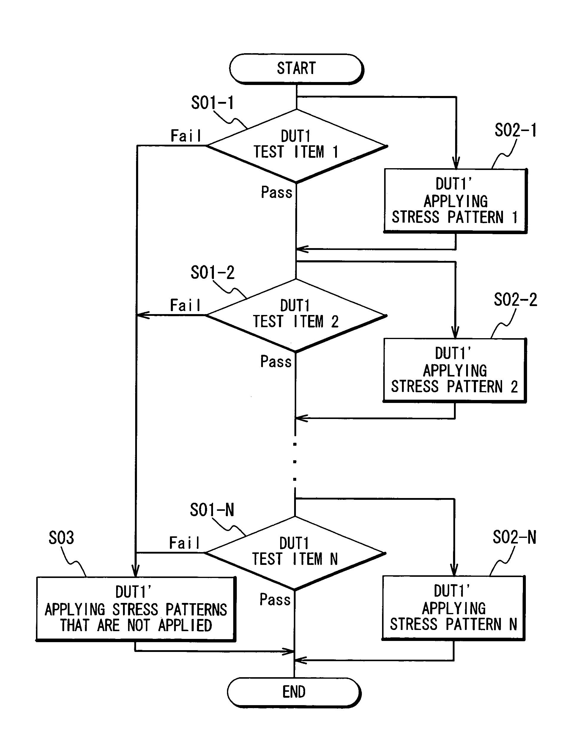
[0022]In the first embodiment, the method for the burn-in test according to the present invention is applied to a wafer level burn-in technique. The method for the wafer level burn-in test in this embodiment schematically executes a burn-in of a second semiconductor device during the execution of an operation test of a first semiconductor device. After the burn-in and the operation test are completed, the burn-in of a third semiconductor device and the operation test of the second semiconductor device are executed. The method for the wafer level burn-in test executing the burn-in and the operation test through the foregoing procedure substantially improves the throughput of the burn-in and the operation test, and effectively reduces the time necessary for a wafer level burn-in inspection.

[0023]The facilities and apparatuses to attain the above-mentioned method for the wafer level burn-in test and its detailed procedure will be disclosed below.

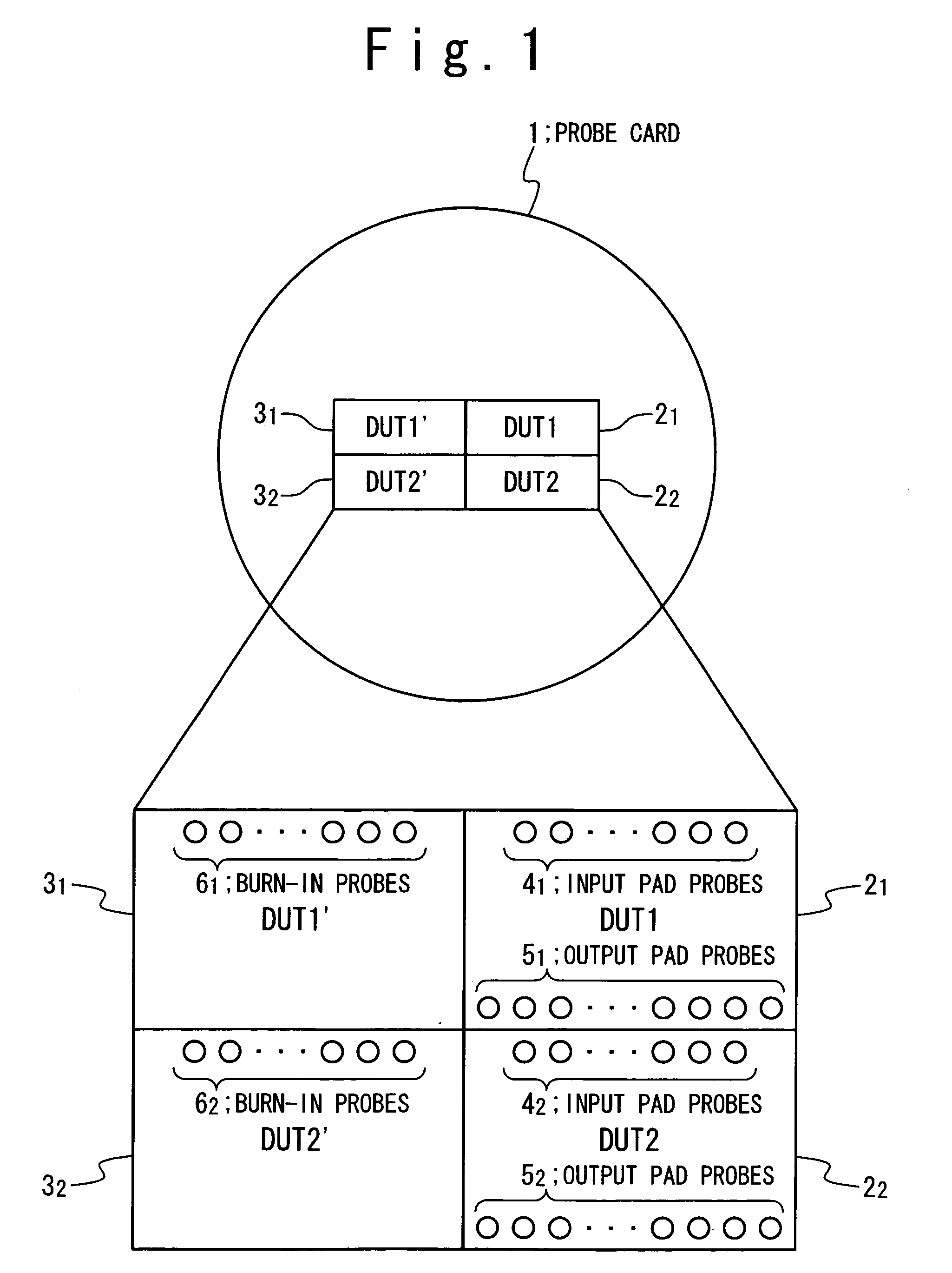
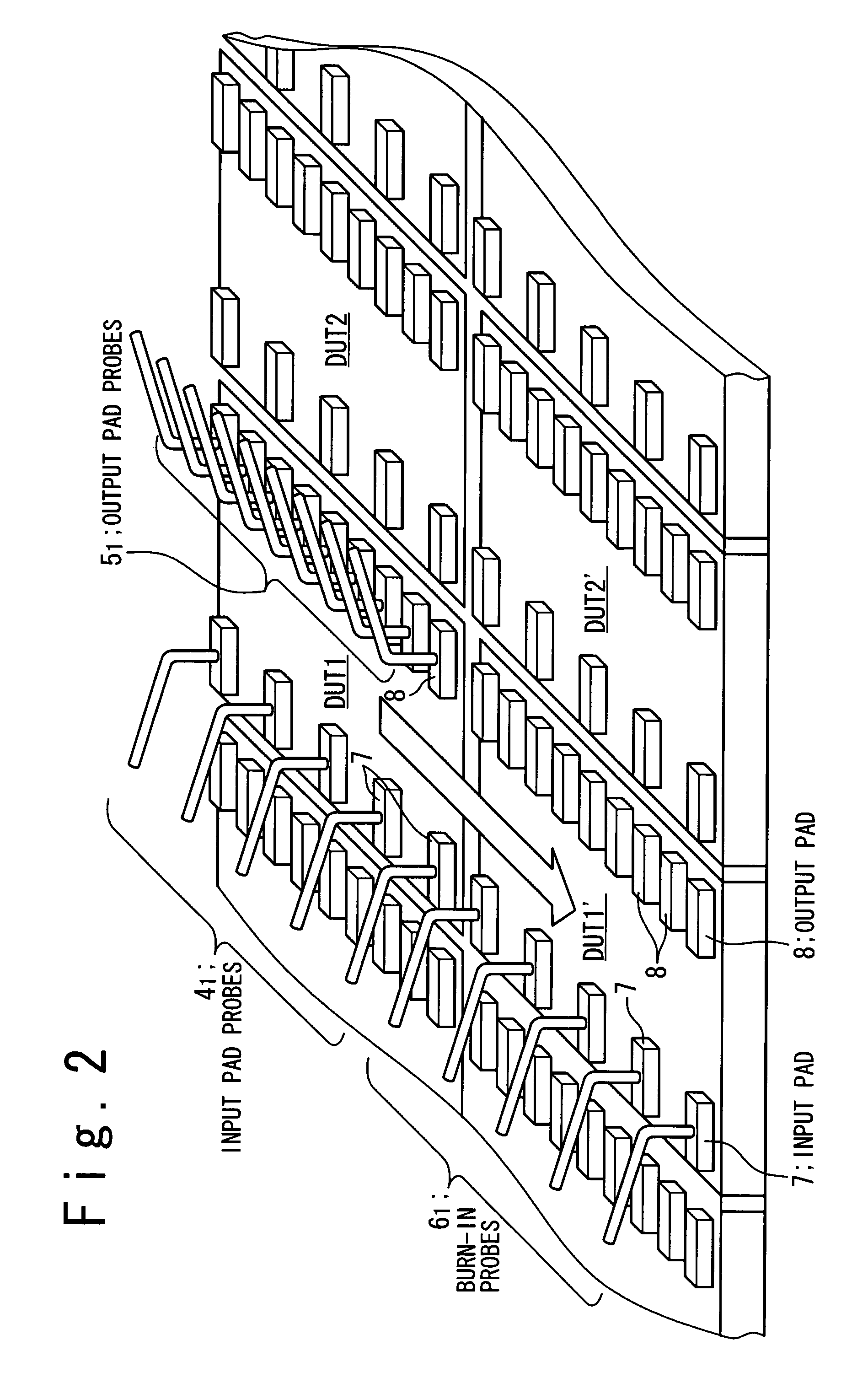
[0024]FIG. 1 is a conceptual view showin...

second embodiment

[0053]In the second embodiment, the present invention is applied to the burn-in of the semiconductor device employing the TAB.

[0054]FIG. 6 is a conceptual view showing the structure of the semiconductor device in which the TAB is employed in the packaging. The semiconductor devices DUT1 and DUT1′ are joined to a carrier tape 21. Input pads 22 and output pads 23 are formed on the carrier tape 21. The input pads 22 are the pads used to supply the input signals from the outside to the semiconductor devices DUT1 and DUT1′. The input pads 22 are connected through input pattern wires 24 to the semiconductor devices DUT1 and DUT1′. On the other hand, the output pads 23 are the pads used to output the output signals from the semiconductor devices DUT1 and DUT1′, and the output pads 23 are connected through output pattern wires 25 to the semiconductor devices DUT1 and DUT1′.

[0055]FIG. 7 is a conceptual view showing a configuration of a probe card 1′ used in the method of the burn-in test in ...


PUM


Abstract

A method for a burn-in test includes steps (a) and (b). In the step (a), an operation test of a first semiconductor device is executed through first probes provided on a probe card. In the step (b), a stress is applied to a second semiconductor device through second probes provided on the probe card while the operation test is executed.

Description

BACKGROUND OF THE INVENTION[0001]1. Field of the Invention[0002]The present invention relates to a method for a burn-in test.[0003]2. Description of the Related Art[0004]Various mounting techniques are developed to attain a high density mounting of a semiconductor device. For example, TAB (Tape Automated Bonding) or COF (Chip on Film) is often employed to mount the semiconductor device on a carrier tape for a liquid crystal driver IC. Also, CSP (Chip Size Packaging) or MCP (Multi-Chip Package) is often employed for a portable apparatus IC.[0005]One of items to be considered in employing the foregoing mounting techniques is an execution method for a burn-in. To secure KGD (Known Good Die) having a high reliability, it is essentially necessary to execute the burn-in. However, when the mounting technique such as the TAB, COF, CSP or MCP is employed, the burn-in using a burn-in board can not be executed unlike in the case of a typical semiconductor device. For the mounting technique suc...

Claims


Application Information

Patent Timeline
Patent Type & Authority Patents(United States)
IPC IPC(8): G01R31/26
CPCG01R31/287G01R31/2863H01L22/00G01R31/26
Inventor SASAKI, SUGURU
Owner RENESAS ELECTRONICS CORP
Why Eureka
Try Eureka