Memory device and method for burn-in test

a memory device and burn-in test technology, applied in semiconductor devices, digital storage, instruments, etc., can solve the problems of low stress efficiency, defective devices, and inability to repair with laser and re-assemble, so as to reduce burn-in test time and increase burn-in test efficiency

Active Publication Date: 2006-03-09
ELITE SEMICON MEMORY TECH INC
View PDF2 Cites 0 Cited by
  • Summary
  • Abstract
  • Description
  • Claims
  • Application Information

AI Technical Summary

Benefits of technology

[0017] An object of the present invention is to provide a memory device and a burn-in test circuit capable of maintaining the stress condition when fatal defects exist during a burn-in test.
[0021] A further object of the present invention is to provide a memory device, a burn-in test circuit, and a method capable of increasing the burn-in test efficiency and reducing the burn-in test time.
[0025] The predetermined sub-array current value is related to the number of spare word lines. Each single word line leak-current limited unit is connected to one word line and limits the current in the word line to the predetermined word line current value. Because the current flowing in one word line is limited, the voltage source is capable of supplying sufficient voltage to stress all word lines. Therefore, the memory device is capable of maintaining the stress condition when fatal defects exist during a burn-in test.
[0030] Next, a word line stress voltage is applied to the word lines. Next, a cell plate voltage is applied to the storage capacitors of the array of memory cells. Next, a bit line stress voltage is applied to the bit lines. The method includes disabling the sense amplifier control signal and turning on all sub-array word line drivers and bit switches. The method is capable of increasing the burn-in test efficiency and reducing the burn-in test time.

Problems solved by technology

The screened devices, if defective, cannot be repaired with a laser and re-assembled.
Volume production is therefore more expensive.
The stress efficiency is low if the burn-in test time cannot be increased, especially for the high-density new generation memory device.
Similar problems arise for a column address to access stored data or to write in new data.
For example, a word line defect is burned out successfully during the burn-in test, or there are inherent word line related defects.
Both result in a leakage path on the word line.
In an extreme case, this defect causes the word line to short directly to the ground, so the leakage current is too large to be supplied by the voltage source.
When the stress voltage is reduced, the electric field across gate oxide film becomes insufficient.
This method cannot screen out the defects relative to an adjacent bit line.
Another disadvantage is that the separate voltage levels have different responses to ground noise, which is always something against bit line signal sensing in normal operation.

Method used


Image

  • Memory device and method for burn-in test
  • Memory device and method for burn-in test
  • Memory device and method for burn-in test

Examples


Embodiment Construction

[0043] Reference will now be made in detail to the present preferred embodiments of the invention, examples of which are illustrated in the accompanying drawings. Wherever possible, the same reference numbers are used in the drawings and the description to refer to the same or like parts.

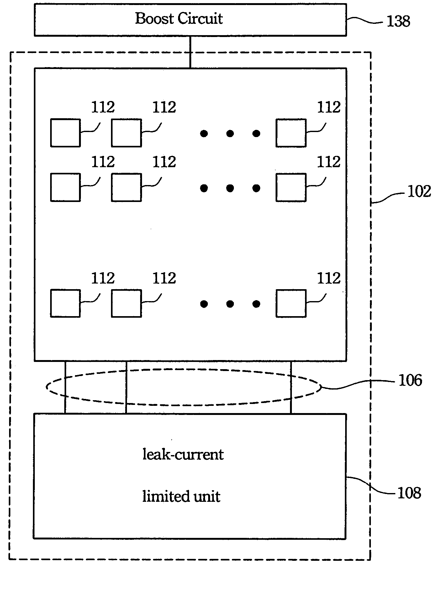
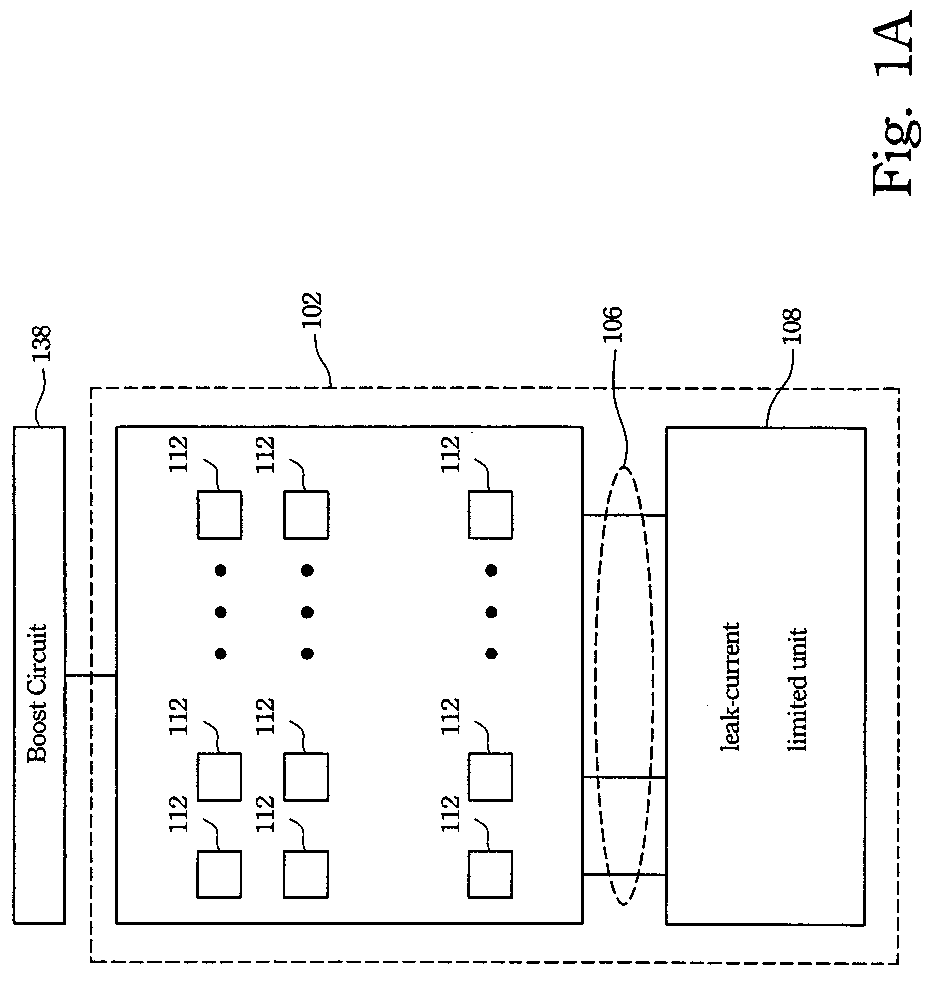
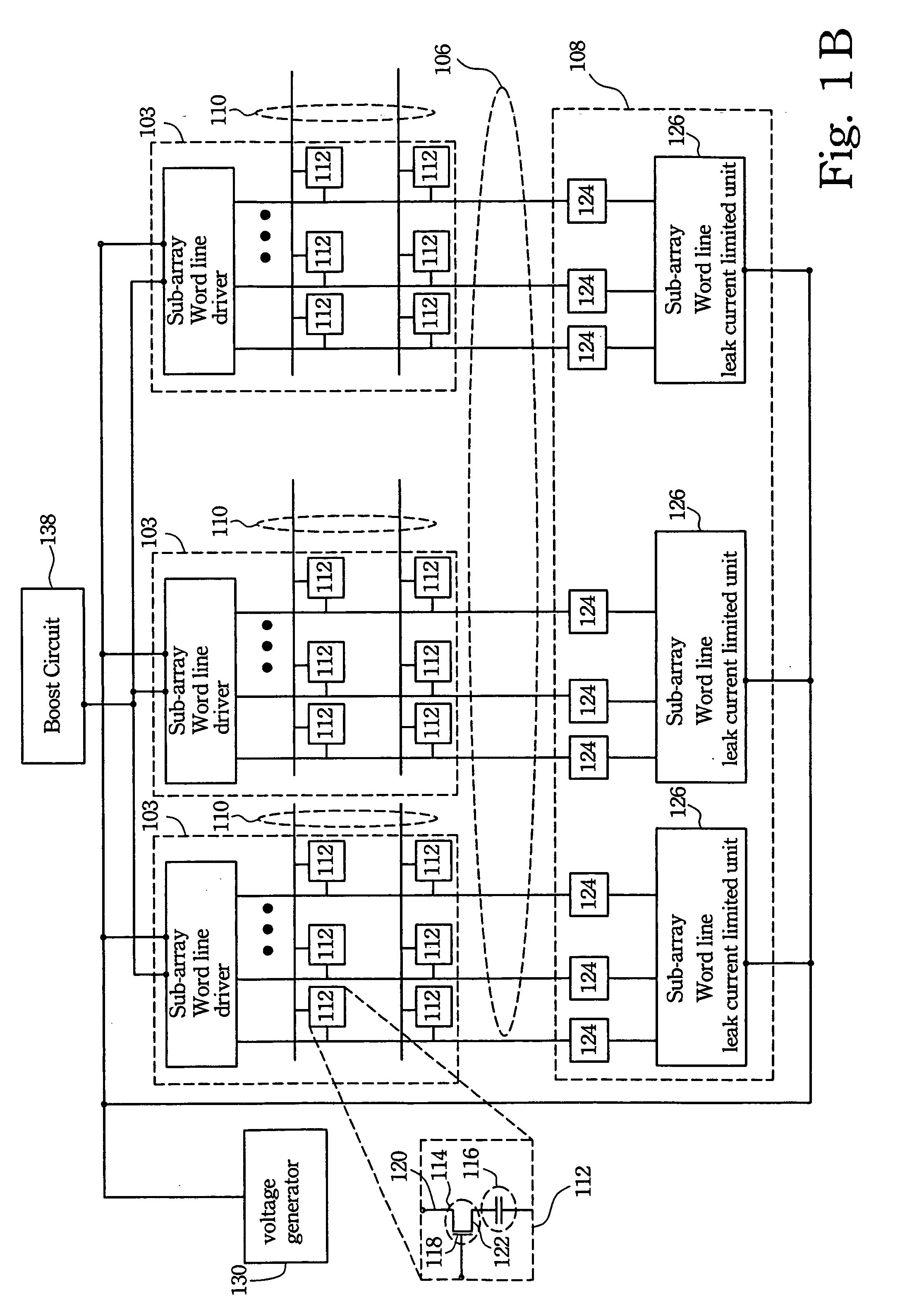
[0044]FIG. 1A is a block diagram illustrating the preferred embodiment of the invention. FIG. 1B is a block diagram illustrating the detail structure of the preferred embodiment of the invention. With reference to FIG. 1A and FIG. 1B, the memory device 102 includes an array of memory cells 112, a plurality of word lines 106, a plurality of bit lines 110, and a leak-current limited unit 108.

[0045] Each word line 106 is connected to a column of the array of memory cells 112. Each bit line 110 is connected to a row of the array of memory cells 112. The leak-current limited unit 108 is connected to the memory array 102 via the plurality of word lines 106.

[0046] The memory cell 112 is, for example, a ...


PUM


Abstract

A memory device and a method for burn-in test are described. The memory device has a plurality of sub-array word line leak-current limited units and a plurality of single word line leak-current limited units. They are used to limit the current in each word line to a predetermined word line current value. In burn-in test mode, the output of a word line driver is kept in a high impedance state. The bit line stress voltage is applied to the row of memory cells through a normal read-write path. A voltage generator for generating a substantially stable voltage is also provided. In burn-in test mode, the even word lines and the odd word lines are grouped separately and the word line stress voltage is applied to the even word lines and to the odd word lines alternately.

Description

BACKGROUND [0001] 1. Field of Invention [0002] The present invention relates to a memory device. More particularly, the present invention relates to a memory device for a burn-in test and a method for screening out defective dynamic random access memory (DRAM) cells in the wafer state. [0003] 2. Description of Related Art [0004] In general, a burn-in test is performed on a semiconductor memory device to prevent reliability problems, and more specifically, after the device has been assembled or packaged. The screened devices, if defective, cannot be repaired with a laser and re-assembled. Volume production is therefore more expensive. The bum-in test is usually performed at a high voltage and high temperature; the semiconductor memory device is operated in read or write mode to screen out possible existent defects in, for example, the gate oxide film of the cell transistor, the storage node and the p / n junctions, the cell capacitor insulator film, the adjacent word lines, the adjacen...

Claims


Application Information

Patent Timeline
Patent Type & Authority Applications(United States)
IPC IPC(8): G11C8/02G11C29/00G11C29/12H01L23/58
CPCG11C11/401G11C29/006G11C2029/1202G11C29/12005G11C29/12
Inventor CHOU, MIN-CHUNG
Owner ELITE SEMICON MEMORY TECH INC
Why Eureka
Try Eureka