Memory device for pre-burning test and method therefor

A memory and memory array technology, applied in static memory, instruments, etc., can solve problems such as failure to detect defects and poor bit line signal detection

Active Publication Date: 2008-09-24
ELITE SEMICON MEMORY TECH INC
View PDF12 Cites 0 Cited by
  • Summary
  • Abstract
  • Description
  • Claims
  • Application Information

AI Technical Summary

Problems solved by technology

This method cannot detect defects that are correlated between adjacent bit lines
Another disadvantage is that the separate voltage levels respond differently to ground noise signals, which in normal operation can have a bad effect on bit line signal detection

Method used


Image

  • Memory device for pre-burning test and method therefor
  • Memory device for pre-burning test and method therefor
  • Memory device for pre-burning test and method therefor

Examples


Embodiment Construction

[0038] The present invention is described in detail in terms of practical embodiments, and the examples in the embodiments are described with reference to the drawings. The same reference numerals in the drawings and the specification represent the same or similar parts.

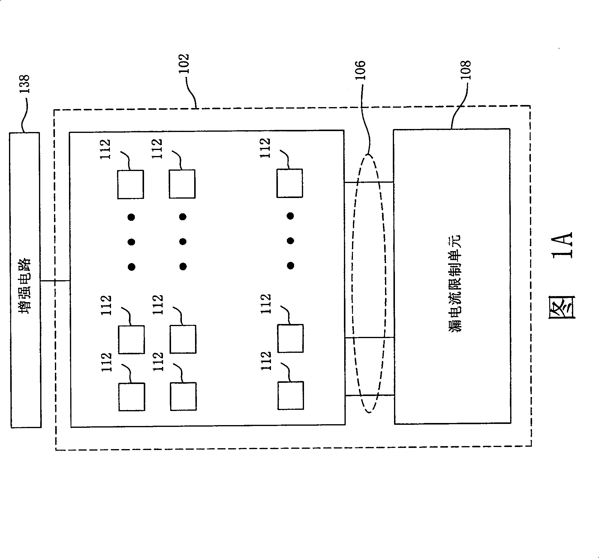
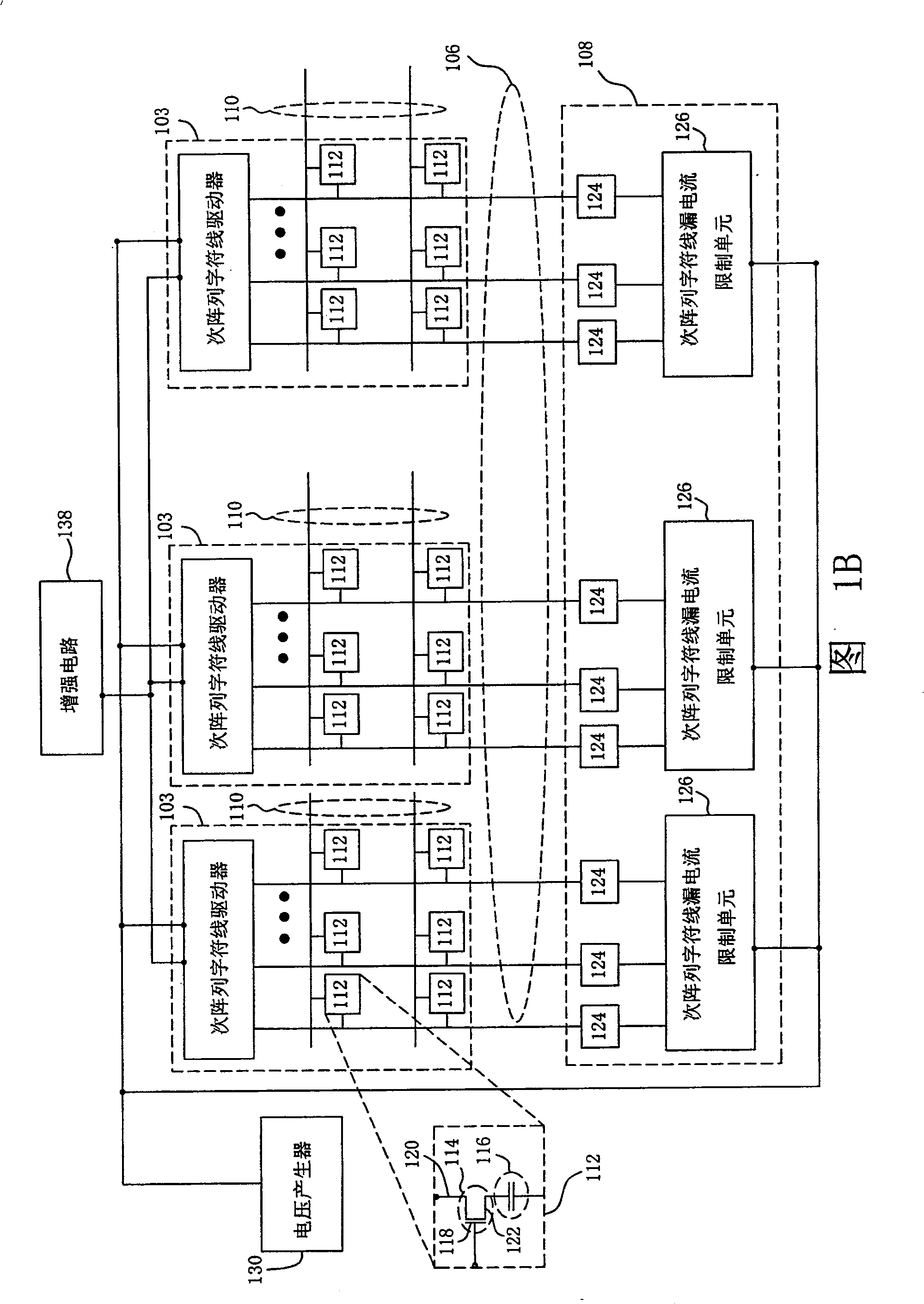
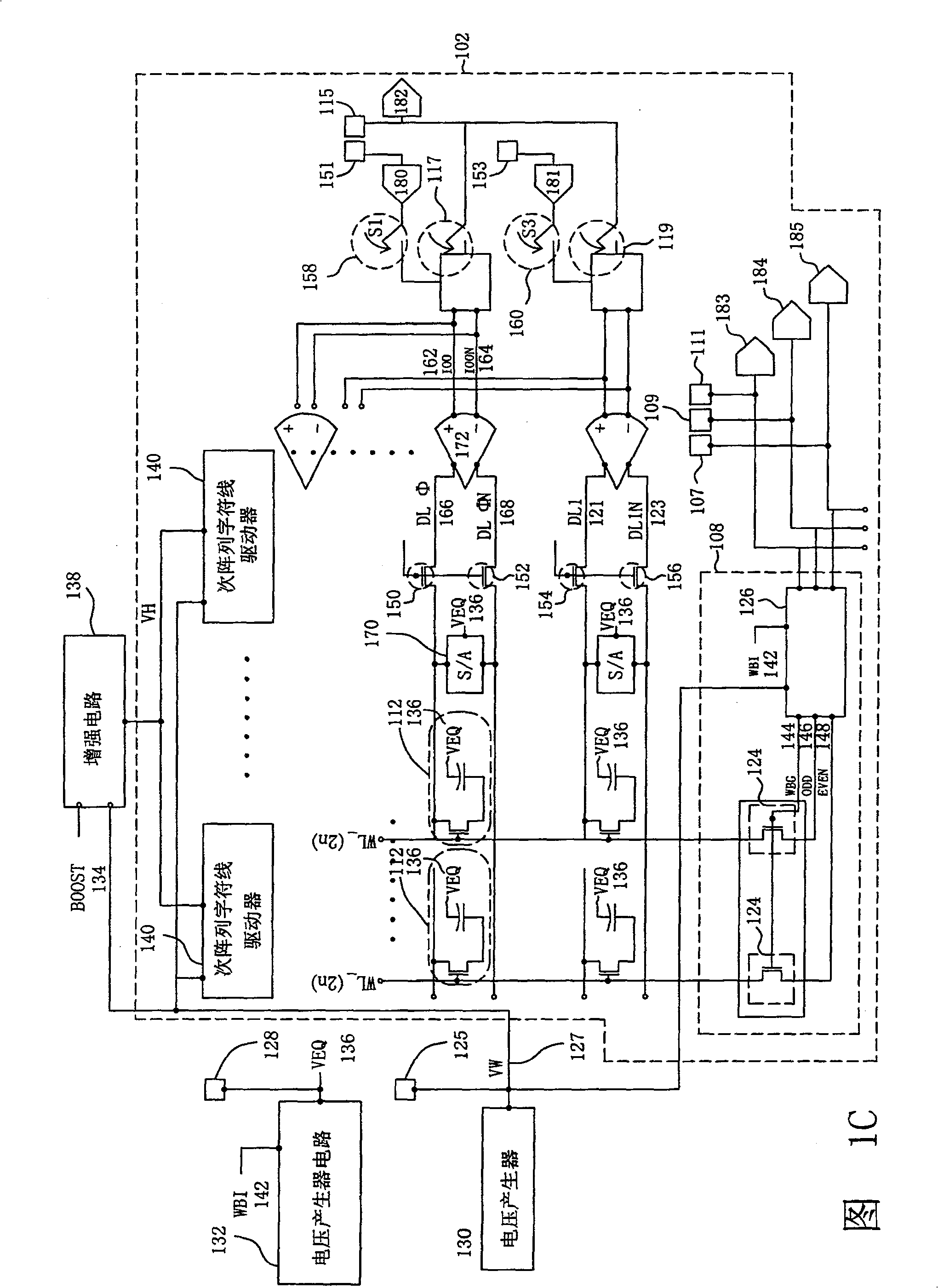
[0039] FIG. 1A shows a block diagram of a preferred embodiment of the present invention. FIG. 1B is a block diagram showing the detailed structure of a preferred embodiment of the present invention. Referring to FIGS. 1A and 1B , the memory device 102 includes a memory array 112 , a plurality of word lines 106 , a plurality of bit lines 110 and a leakage current limiting unit 108 .

[0040] Each word line 106 is connected to a row in the memory array 112 . Each bit line 110 is connected to a column in the memory array 112 . The leakage current limiting unit 108 is connected to the memory array 112 via a plurality of word lines 106 .

[0041] The memory 112 is, for example, a DRAM cell. Please refer to F...


PUM


Abstract

This invention relates to a prefire testing memory device and its method, which comprises multiple sub-array character, drain current limit units and multiple single character drain current limit units. The device uses an intended character line current rating to limit every current through every character line. In the prefire test, character line drive output is in high-impedance state. Bit line forcing voltage is pressurized in a line of memory via normal read-write path. In prefire testing mode, even number and odd number character lines are sub-grouped and character line forcing voltage added on the even and odd character line in alternatively switching way.

Description

【Technical field】 [0001] The present invention relates to a memory device, and more particularly to a memory device for burn-in testing and a method for detecting defective memory in dynamic random access memory (DRAM) at the wafer level. 【Background technique】 [0002] Generally, the burn-in test is performed on a semiconductor memory to prevent reliability problems. More precisely, after the memory has been assembled or packaged. If the detected components are defective, they cannot be repaired or re-assembled by laser. Therefore, mass production can be very expensive. The burn-in test is usually carried out under high voltage and high temperature, and the semiconductor storage element is operated in the state of reading or writing to detect possible problematic defects, such as the gate layer of the transistor of the memory element, the storage node, and the p / n junction , the insulating layer of the capacitor, adjacent word lines, adjacent bit lines, word lines, and b...

Claims


Application Information

Patent Timeline
Patent Type & Authority Patents(China)
IPC IPC(8): G11C29/00
Inventor 周敏忠
Owner ELITE SEMICON MEMORY TECH INC
Why Eureka
Try Eureka