

Semiconductor package and its manufacturing method
a technology of semiconductors and packaging, applied in the direction of semiconductor devices, semiconductor/solid-state device details, electrical equipment, etc., can solve the problems of reducing the overall size of the package, affecting the signal processing capability of the package, and requiring the use of die paddles, etc., to achieve the effect of increasing the signal processing capability
- Summary
- Abstract
- Description
- Claims
- Application Information
AI Technical Summary
Benefits of technology
Problems solved by technology
Method used
Image

Examples
first embodiment
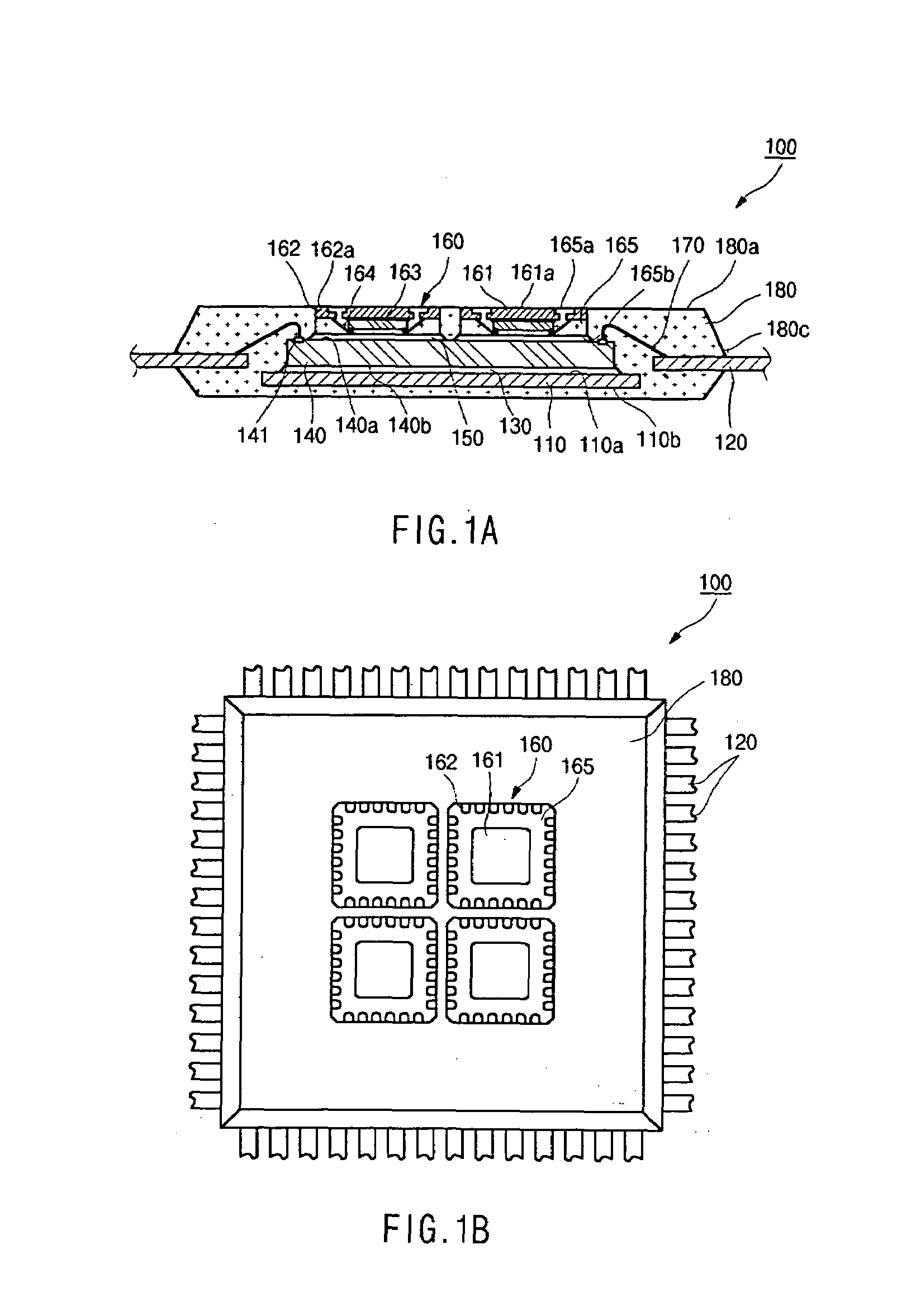
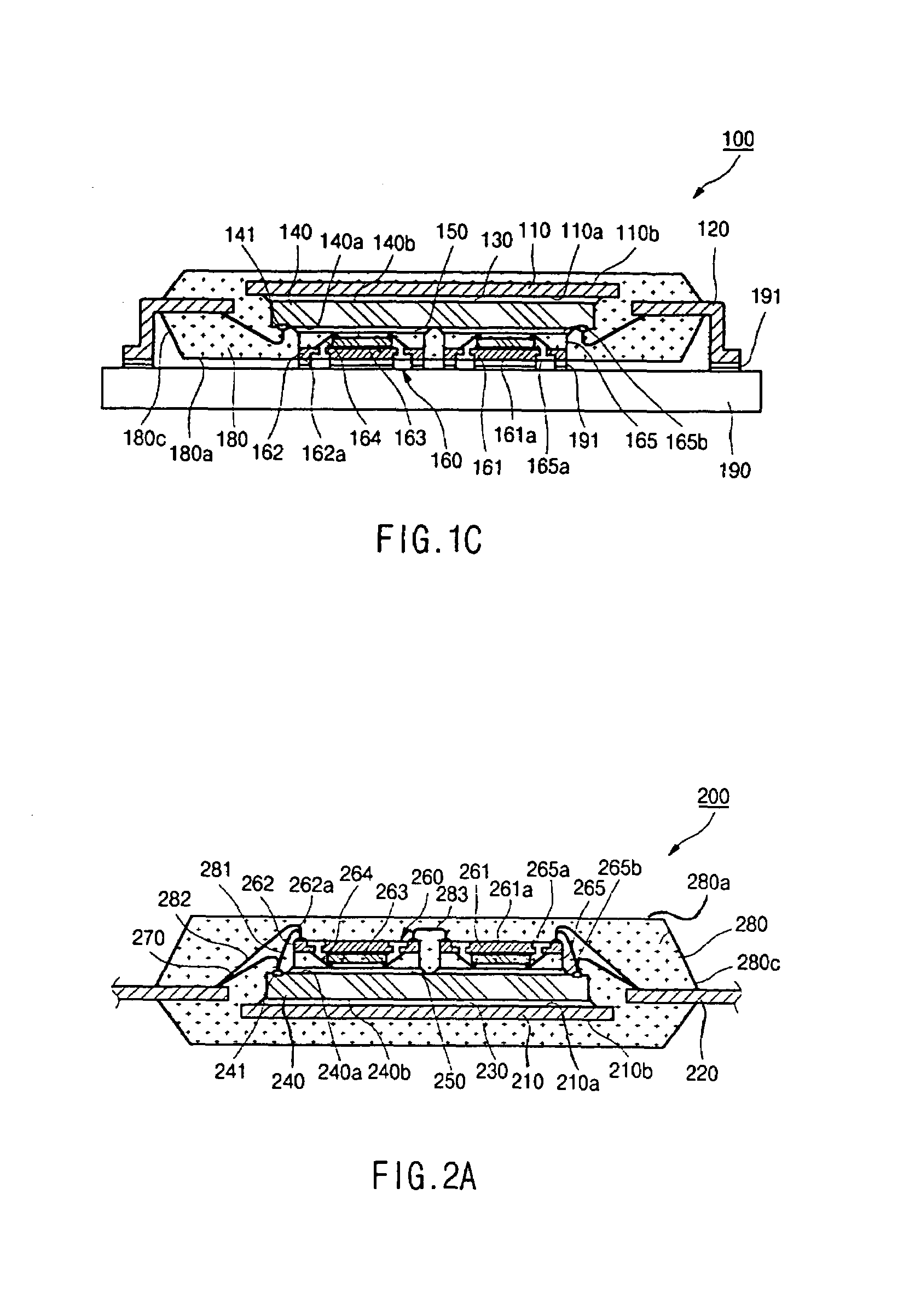
[0024]Referring now to the drawings wherein the showings are for purposes of illustrating preferred embodiments of the present invention only, and not for purposes of limiting the same, FIGS. 1A–1C illustrate a semiconductor package 100 constructed in accordance with the present invention. The semiconductor package 100 comprises a leadframe L / F (shown in FIG. 4A) which itself includes a die paddle 110 having a generally quadrangular (e.g., square, rectangular) configuration. The die paddle 110 defines a generally planar upper surface 110a and an opposed, generally planar lower surface 110b. Those of ordinary skill in the art will recognize that the die paddle 110 need not necessarily have a quadrangular shape, and may alternatively have a differing shape such as polygonal shape.
[0025]In addition to the die paddle 110, the leadframe L / F includes a plurality of leads 120 which are arranged along the periphery of the die paddle 110. The leads 120 are preferably segregated into four set...
second embodiment
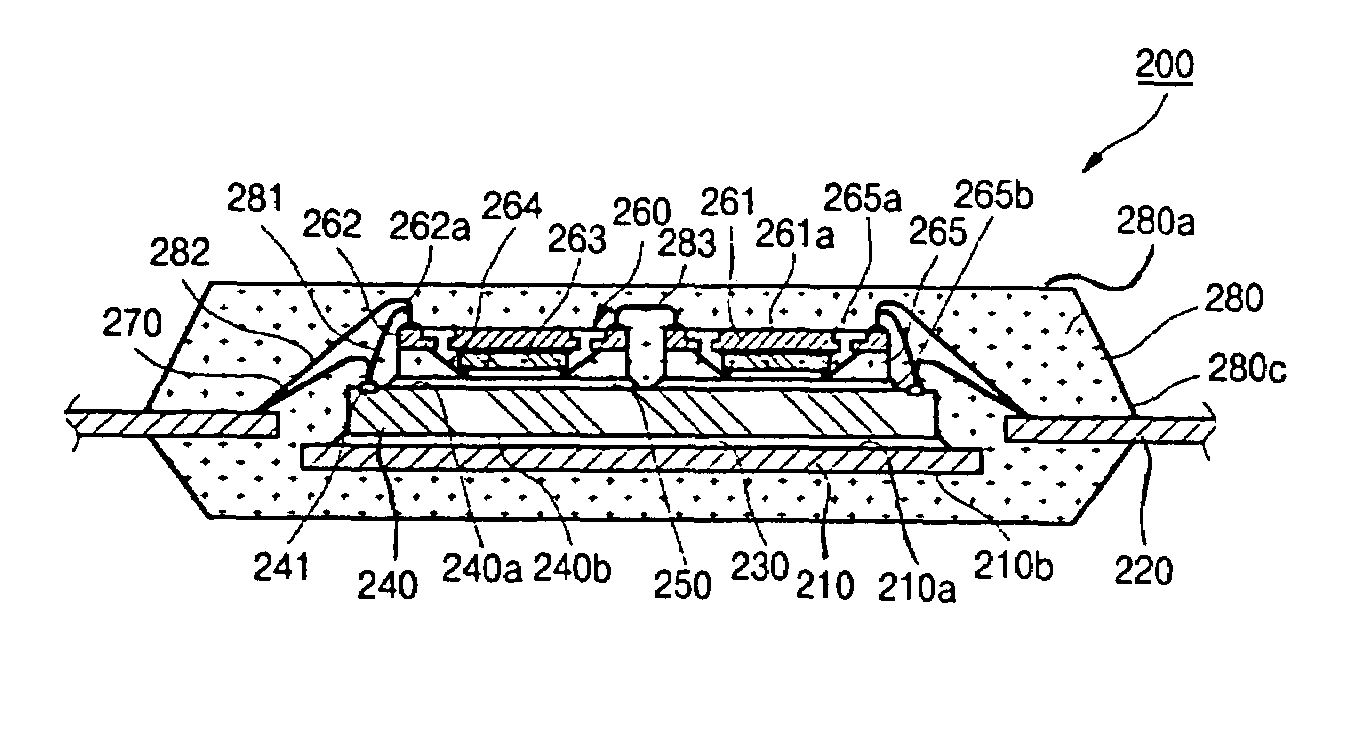
[0038]Referring now to FIGS. 5A–5E, there is shown an exemplary sequence of steps which may be used to facilitate the fabrication of the semiconductor package 200 of the In the initial step of the sequence, the leadframe L / F is provided, such leadframe L / F including the die paddle 210 and leads 220 (FIG. 5A). Thereafter, the semiconductor die 240 is attached to the upper surface 210a of the die paddle 210 through the use of the adhesive agent 230 (FIG. 5B). The inner package(s) 260 are then attached to the upper surface 240a of the semiconductor die 240 through the use of the adhesive agent 250 (FIG. 5C).
[0039]Subsequent to the attachment of the inner package(s) 260 to the upper surface 240a of the semiconductor die 240, a wire bonding step is completed wherein the conductive wires 270, 281, 282, 283 are used to establish electrical interconnections between the various components of the semiconductor package 200 in the above-described manner (FIG. 5D). Thereafter, the package body ...
third embodiment
[0044]Referring now to FIGS. 6A–6E, there is shown an exemplary sequence of steps which may be used to facilitate the fabrication of the semiconductor package 300 of the In the initial step of the sequence, the leadframe L / F is provided, such leadframe L / F including the die paddle 310 and leads 320 (FIG. 6A). Thereafter, the semiconductor die 340 is attached to the upper surface 310a of the die paddle 310 through the use of the adhesive agent 330 (FIG. 6B). The inner package(s) 360 having the above-described structural attributes are then attached to the upper surface 340a of the semiconductor die 340 in the aforementioned manner through the use of the adhesive agent 350 (FIG. 6C).
[0045]Subsequent to the attachment of the inner package(s) 360 to the upper surface 340a of the semiconductor die 340, a wire bonding step is completed wherein the conductive wires 370, 381, 382, 383 are used to electrically interconnect various components of the semiconductor package 300 to each other in...
PUM
 Abstract
Description
Claims
Application Information