Process to improve carrier mobility of organic semiconductor

a technology of organic semiconductor and carrier mobility, applied in the direction of basic electric elements, electrical apparatus, semiconductor devices, etc., can solve the problems of low carrier mobility and high driving voltage, bottlenecks choking further research, and low carrier mobility, so as to improve the carrier mobility of organic semiconductor

Inactive Publication Date: 2007-05-01
IND TECH RES INST
View PDF1 Cites 15 Cited by
  • Summary
  • Abstract
  • Description
  • Claims
  • Application Information

AI Technical Summary

Benefits of technology

[0008]It is a primary object of the invention to provide a process to improve carrier mobility of organic semiconductor by forming an interlayer of a specific polymer, that the process of the invention is simple and low-cost.
[0009]Another object of the invention is to provide a process to improve carrier mobility of organic semiconductor by coating a specific polymer as the interlayer thereof for enabling the coating condition to be easily controlled and the specific polymer to have more choices.
[0010]Yet, another object of the invention is to provide a process to improve carrier mobility of organic semiconductor having no evaporation during the process, so that the resulting organic semiconductor is stable, and thus the throughput yield and the stability of OTFT are both enhanced.

Problems solved by technology

Although the organic thin film transistor has the advantages as described above, there are still some bottlenecks choking the further research, such as low carrier mobility and high driving voltage.
The low carrier mobility limits the development and application of OTFT.
In this regard, the material of U.S. Pat. No. 6,433,359 has a limited choice, and the condition of the precursor reacting with the dielectric layer is not easily controlled.
In addition, evaporation deposition is used for forming the interlayer of the U.S. Pat. No. 6,433,359 that the SAM is easily evaporated during the manufacturing process causing the same to have unstable quality.
Form the above description, the conventional process of OTFT has the following drawbacks:1. The forming of interlayer in the conventional process of OTFT is complicated and time-consuming that the high manufacture cost of the conventional process is increased so as to reduce it commercial competitiveness.2. The interlayer can be formed only when the precursor can react with the dielectric layer in the conventional process of OTFT, therefore the material of the interlayer has a limited choice, and the condition of the precursor reacting with the dielectric layer is not easily controlled.3. The interlayer is formed by evaporation deposition so that the SAM is easily evaporated during the manufacturing process causing the same to have unstable quality.

Method used


Image

  • Process to improve carrier mobility of organic semiconductor
  • Process to improve carrier mobility of organic semiconductor
  • Process to improve carrier mobility of organic semiconductor

Examples


Embodiment Construction

[0021]For your esteemed members of reviewing committee to further understand and recognize the fulfilled functions and structural characteristics of the invention, several preferable embodiments cooperating with detailed description are presented as the follows.

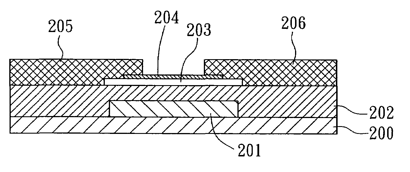
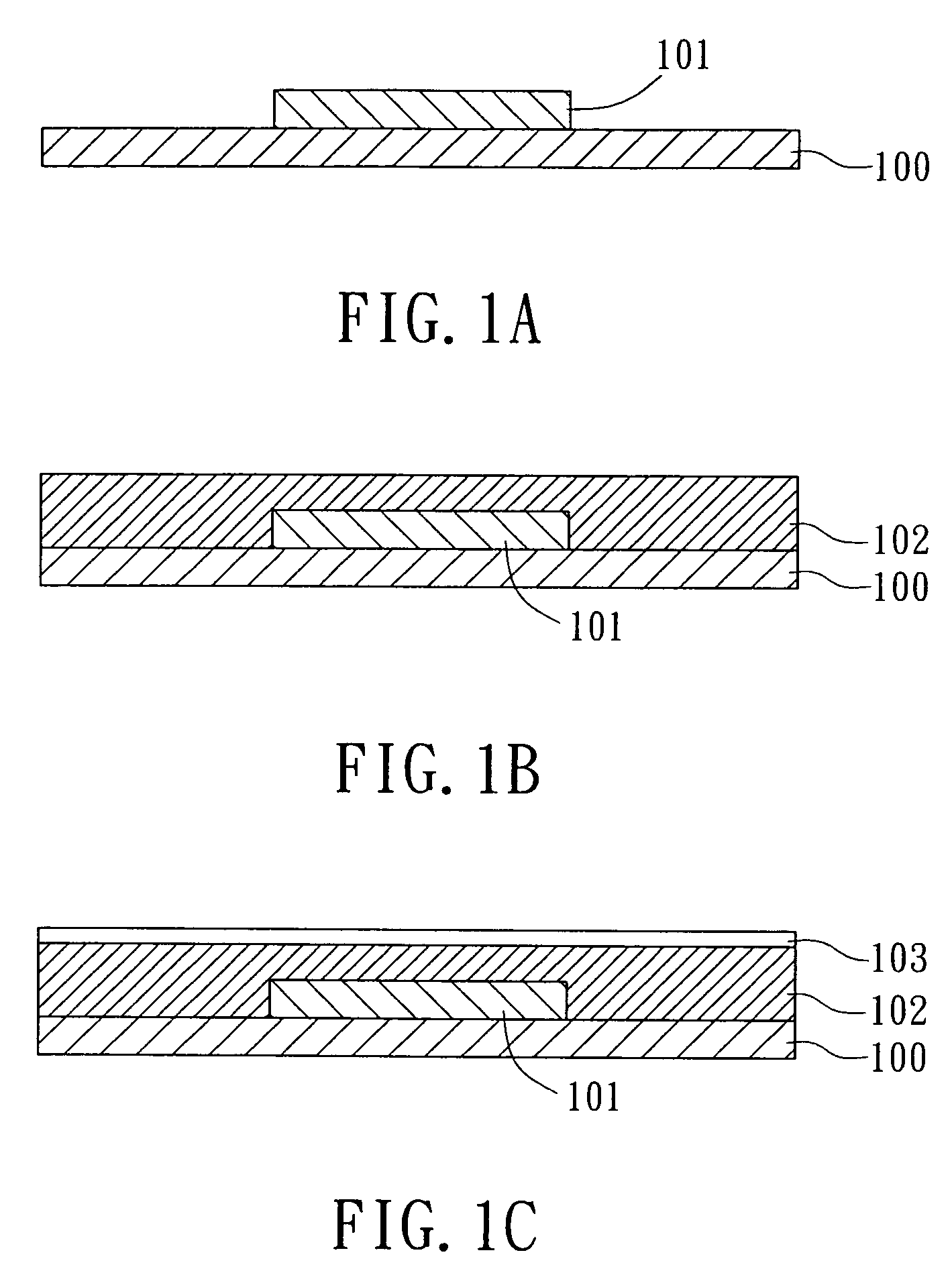
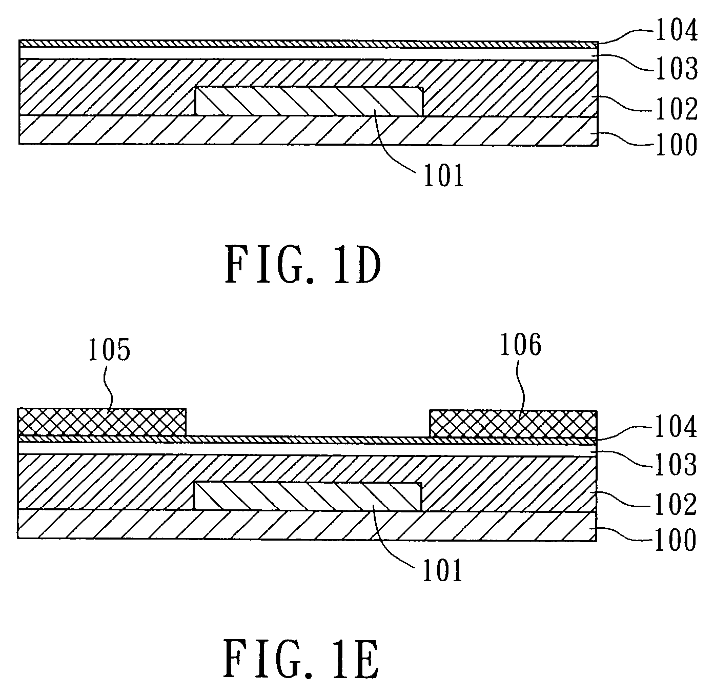
[0022]Please refer to FIG. 1A to FIG. 1E, which are schematic diagrams of a process to improve carrier mobility of organic semiconductor according to a first preferred embodiment of the invention. As seen in FIG. 1A, a substrate 100 is pre-processed and cleaned to remove tiny particles and organics thereon. Thereafter, a gate 101 of metal or conductive polymer such as Cr or ITO is formed on the substrate 100 which can be made of silicon wafer, glass, quartz, plastic or other flexible material.

[0023]As shown in FIG. 1B, an insulator layer 102 is formed on the gate 101 and the substrate 100. The insulator 102 can be made of non-organic material, polymer or high-K material for insulating the OTFT.

[0024]Referring to 1C, an interl...


PUM


Abstract

The invention related to a process for improving carrier mobility of organic semiconductor, comprising the steps of: forming a gate on a substrate; forming an insulator layer on the substrate and the gate; coating polyimide on the insulator layer to form an interlayer; forming an active layer on the interlayer; and forming a source and a drain.

Description

FIELD OF THE INVENTION[0001]The invention relates to a process for improving carrier mobility of organic semiconductor, and more particularly, to a process capable of improving carrier mobility of organic semiconductor by adding an interlayer to an organic thin film transistor (OTFT).BACKGROUND OF THE INVENTION[0002]An organic thin film transistor (OTFT) is made of organic conjugated polymer or oligoanolone. Compared with a conventional non-organic transistor, the OTFT can be constructed at a lower temperature, and thus the substrate of the OTFT can be a plastic substrate which is lighter, thinner and cheaper than the glass substrate of the conventional non-organic transistor. In addition, the organic thin film transistor can employ a simpler manufacture process that doesn't require certain high precision technique and equipment. In this regard, the OTFT are of great potential and interest for further development. Although the organic thin film transistor has the advantages as descr...

Claims


Application Information

Patent Timeline
Patent Type & Authority Patents(United States)
IPC IPC(8): H01L51/40H01L21/84H01L51/00H01L51/05
CPCH01L51/0533H01L51/0545H10K10/476H10K10/466
Inventor HU, TARNG-SHIANGHO, JIA-CHONGHUANG, LIANG-YINGLIN, WEI-LING
Owner IND TECH RES INST
Why Eureka
Try Eureka